Introduction
The main goal of this documentation is to describe how to program the modules of the MCXA153 microcontroller directly through its registers, instead of using driver functions. This is done by providing a basic example for each module and an assignment on top of that example. The hardware required for these assignments is an FRDM-MCXA153 development board.
There are also additional assignments to verify the knowledge acquired. These are marked with Assignment. These extra assignments require additional hardware, which is conveniently available on a dedicated Shield V3.
The content of this site can also be downloaded as a single PDF as follows:
- Add print_page.html at the end of the URL
- CTRL+P
- Save as PDF
Prior knowledge and skills
Before starting with these example projects, it is expected that you have the following knowledge and skills:
- Know how to represent numbers in different numbering systems, such as decimal, binary, and hexadecimal.
- Can program in C at the beginners level.
- Know the bitwise operators and what they are used for.
- Know what a register is.
Disclaimer
This content is provided for education and demonstration purpose.
Static documents
This content uses static documents downloaded from several sources. The reason for this is the ability to directly reference paragraphs and pages within these documents, which makes it more convenient to find relevant information. The following documents were downloaded and are part of this content:
- Arm® v8-M Architecture Reference Manual - DDI0553B.x ID15122023
- FRDM-MCXA153 Board User Manual - Rev. 2.0 — 12 February 2025
- FRDM-MCXA153 Schematic diagrams - Rev A1, 28-Aug-2023
- MCX A153, A152, A143, A142 Reference Manual - Rev. 5, 08/2024
- MCXA153, A152, A143, A142 Data Sheet - Rev. 3 — 01/2024
- P3T1755 Product data sheet - Rev. 1.1 — 4 January 2023
- ARM® Cortex®-M for Beginners - White paper - March 2017
Note. You are encouraged to always check if there are new versions of these documents.
KiCad shield template
Myrddin has created a FRDM-MCXA153 shield template for KiCad that fit's both the Arduino headers and the mikroBUS headers at the same time. The shield template is available here.
Contact
This content is part of the microcontroller courses offered by HAN Embedded Systems Engineering.
Have any comments or suggestions? Please let me know by sending me an email.
Hugo Arends
Arnhem - December 2025
Getting Started with VS Code
Resources: ese_general_examples\basics\getting_started
Rather use MCUXpresso-IDE? Check this getting started instead!
Hardware
The NXP FRDM-MCXA153 development board is used in this course.
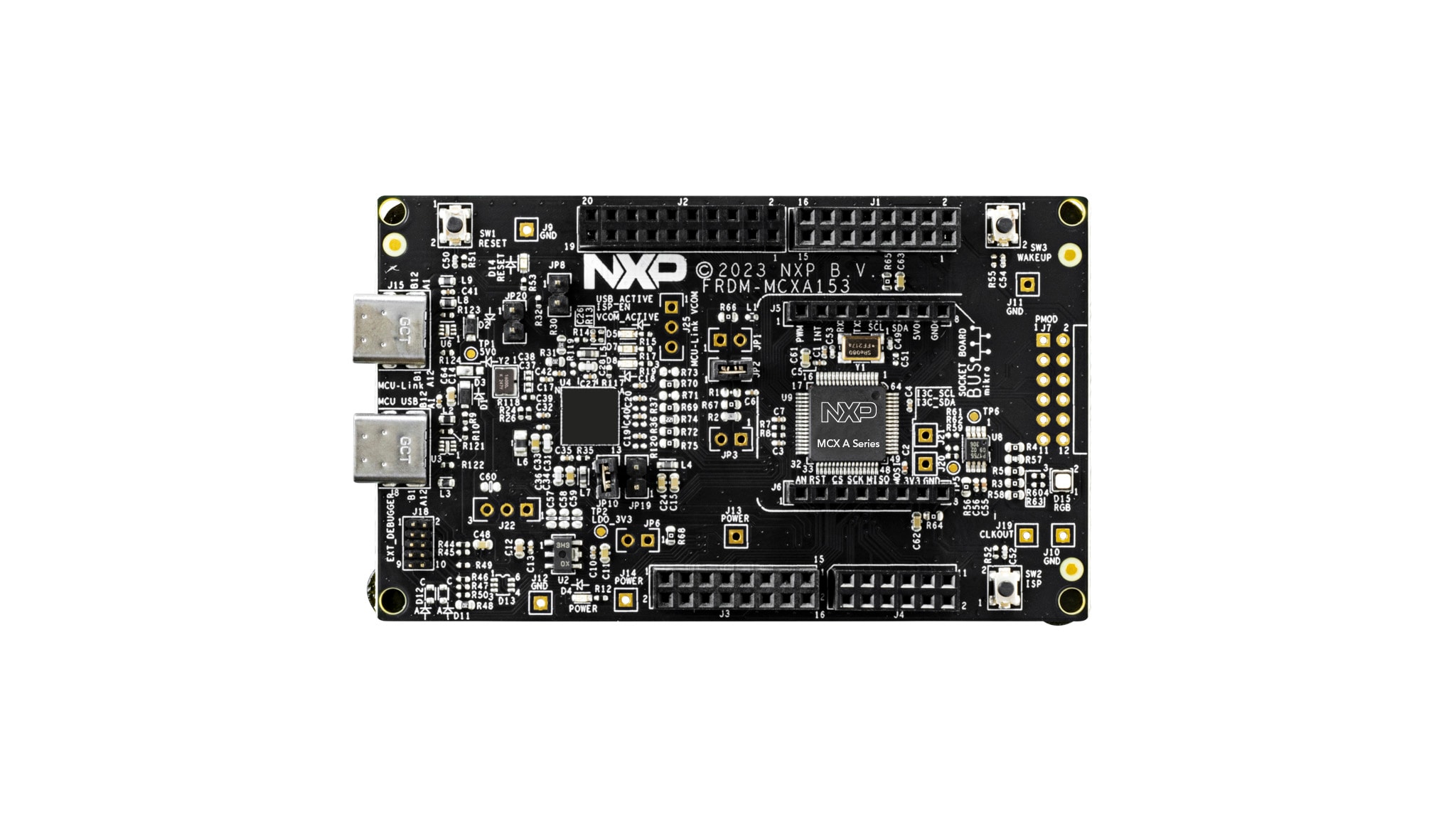
A board overview, product details, documentation and other resources is provided on the NXP website. A board can purchased from ARLE, the NXP website or other electronics suppliers.
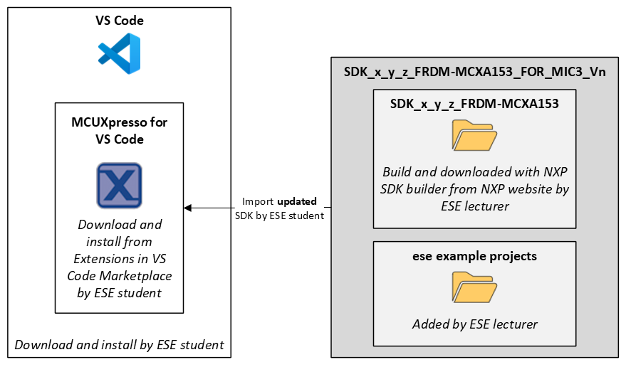
SDE overview
The following diagram shows the tools and dependencies used in the Software Development Environment. A detailed description of where to download and how to configure these tools is given in the rest of this document.
Download and install VS Code
Download and install the latest version of VS Code for your operating system.
Download and install extensions
Download and install the MCUXpresso for VS Code extension.
- Start VS Code
- Install the MCUXpresso for VS Code extension: MCUXpresso for VS Code
Download and install MCUXpresso for VS Code components
After installing the MCUXpresso for VS Code extension, you should be prompted to start the MCUXpresso Installer. If not, click Open MCUXpresso Installer from the Quickstart panel in the MCUXpresso for VS Code extension.
The MCUXpresso Installer looks like this:
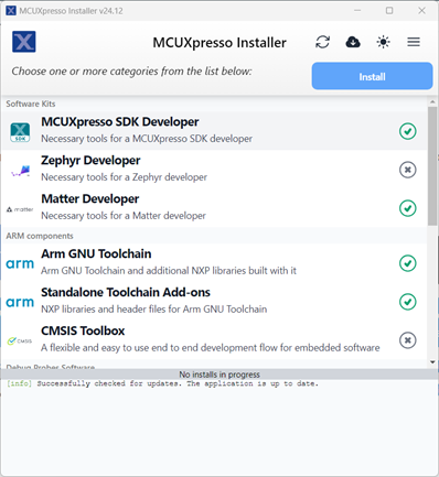
- In this installer, select (at least) the following options:
- MCUXpresso SDK Developer
- ARM GNU Toolchain
- Standalone Toolchain Add-ons
- LinkServer
- SEGGER J-Link
- Click Install
- Close the installer when the installation is finished
Download SDK
The Software Development Kit (SDK) contains source files, project configuration files, documentation, example projects, etc. to help users get started. The updated SDK is available for download as a ZIP archive.
- Download the file SDK_x_y_z_FRDM-MCXA153_FOR_MIC3_Vn.zip from Brightspace.
Note. If you would like to generate your own SDK, without ESE examples, use the SDK builder for the FRDM-MCXA153
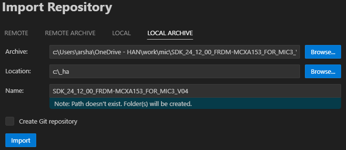
Import SDK in MCUXpresso for VS Code
The downloaded SDK must be imported in MCUXpresso for VS Code.
- Start VS Code
- Select the MCUXpresso for VS Code extension
- Click Import Repository
- Click LOCAL ARCHIVE
- Archive: select the dowloaded SDK
- Location: any location will do, but the path should be as short as possible!
- Name: leave default
- Create Git repository: not checked
The result should look similar to this:
- Click Import
- Wait for the import to finish
After a successful import, the installed SDK is added to the Installed repositories view. For example:
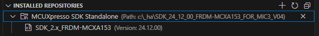
Note. An SDK can be removed by a right-mouse click on the SDK and selecting the appropriate option from the context menu that pops-up.
Import example project in MCUXpresso for VS Code
Import example projects from the SDK in MCUXpresso for VS Code.
- Start VS Code
- Select the MCUXpresso for VS Code extension
- Click Import Example from Repository
- Repository: select the downloaded SDK
- Toolchain: ARM GNU Toolchain (as installed during with MCUXpresso Installer)
- Board: FRDM-MCXA153
- Template: ese_general_examples/basics/ese_general_examples_basics_getting_started
- Name: leave default
- Location: any location will do, but the path should be as short as possible!
The result should look similar to this:
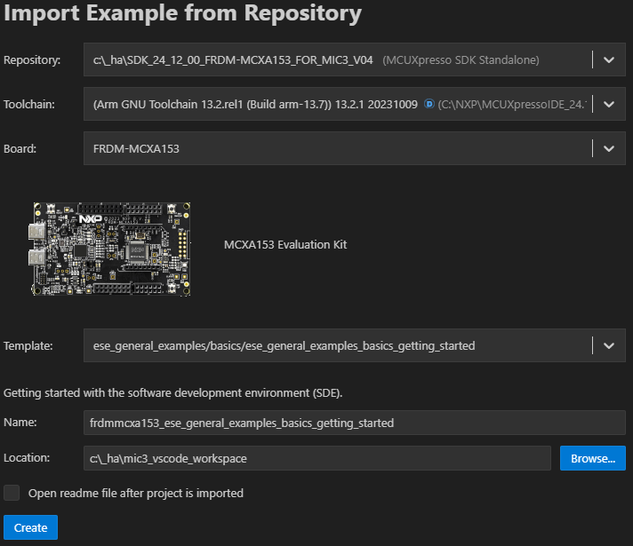
- Click Create
- Wait for the import to finish
MCU-Link firmware update (optional)
The FRDM-MCXA153 board comes with an MCU-Link debug probe. Out of the box, the CMSIS-DAP firmware is installed. Changing the MCU-Link to J-Link firmware is described here.
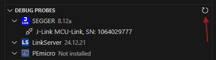
Check board connection
Check if the board is recognized by MCUXpresso for VS Code.
- Connect the FRDM-MCXA153 board to the computer with a USB cable (J15 - MCU-Link)
- Check the Debug probes view to make sure the board is detected. If not, click the Refresh debug probes icon
Build and run the Getting Started application
The imported project is visible in the Projects view in the MCUXpresso for VS Code extension.
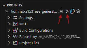
Build and run the project.
- Click the Build icon
- Check the Terminal window for the build to finish successfully
- Click the debug icon
- Wait for the debugger to start
- Click Run, the green LED starts blinking
Note: If you run into build issues, chances are that the path to the project is too long and/or the path contains characters that are not supported by the toolchain (such as hyphens). If so, move the project and the SDK to a location with a shorter path and/or remove unsupported characters from the path.
CMSIS
Resources: none
Goal
To understand what the CMSIS is and how bits are manipulated in registers in C by using CMSIS.
Required hardware
- None
Introduction
This course aims at teaching how to program the modules of the microcontroller directly through its registers, instead of using driver functions. This will be achieved by making use of the Common Microcontroller Software Interface Standard (CMSIS). One subject of this standard is the naming convention for accessing modules. Microcontroller vendors offer CMSIS compliant header and source files that can be added to a project, which is often automated when creating a new project in the SDE of choice. The benefit of using this naming convention is that accessing registers of peripherals in C is done by simple statements. Most microcontroller vendors use names that are also used in their reference manual and/or datasheet.
The CMSIS naming convention for accessing modules is:
MODULE->REGISTER
For example, setting the CTRL register in the SysTick module to zero is done as follows:
SysTick->CTRL = 0x00000000;
Memory mapped IO
All registers in an ARM Cortex-M microcontroller are memory mapped. This means that every registers is located at a 32-bit address. For example, the SySTick->CTRL register in the MCXA153 microcontroller is located at address 0xE000E010. Writing a 32-bit number to this 32-bit address in C can be done as follows:
*((volatile uint32_t *)(0xE000E010)) = 0x00000000;
This is both unreadable and not portable.
Within the SysTick module, there are a total of four 32-bit registers. These registers are called:
- CTRL - Control and Status register
- LOAD - Reload value register
- VAL - Current value register
- CALIB - Calibration register
These register are conveniently grouped in memory. CMSIS takes advantage of the fact that a struct in C is a way to group variables. The registers memory layout of the SysTick module can therefore be represented as a struct:
typedef struct
{
  volatile uint32_t CTRL;   /*!< Offset: 0x000 (R/W)  SysTick Control and Status Register */
  volatile uint32_t LOAD;   /*!< Offset: 0x004 (R/W)  SysTick Reload Value Register */
  volatile uint32_t VAL;    /*!< Offset: 0x008 (R/W)  SysTick Current Value Register */
  volatile const uint32_t CALIB;  /*!< Offset: 0x00C (R/ )  SysTick Calibration Register */
} SysTick_Type;
The base address in memory of this struct will be the address of the first field in the struct, being the CTRL register in this example. And the address of the CTRL register is known, because this is described in the reference manual (or in this case the ARMv8-M documentation, because this is a core register). A more meaningful name for the base address of the module is defined as follows:
#define SysTick ((SysTick_Type *) 0xE000E010 )
This means: SysTick is a pointer pointing to a SysTick_Type struct at address 0xE000E010.
Accessing one of the fields can thus be achieved by using the pointer to a struct
dereference operator: ->
For example:
SysTick->CTRL = 0x00000000;
Cortex-M microcontroller vendors offer comprehensive header files for their devices with CMSIS compliant defines for all the modules and registers.
Bit manipulation
Bits in register are manipulated with the C bitwise operators as follows:
// Assignment: assign a value to all bits in a register
MODULE->REGISTER = (0x00010001);
// Bitwise-or: set bits in a register and leave all others unchanged
MODULE->REGISTER |= (0x00010001);
// Bitwise-and: clear bits in a register and leave all others unchanged
MODULE->REGISTER &= ~(0x00010001);
// Bitwise ex-or: toggle bits in a register and leave all others unchanged
MODULE->REGISTER ^= (0x00010001);
Bit field masks
Instead of using magic numbers (such as 0x00010001 in the example above), CMSIS also provides a convention for accessing bit fields in a register. The convention describes the following three defines for each bit field:
// A 32-bit mask with logic 1s at every location of the bit field
MODULE_REGISTER_BITFIELD_MASK

// The bit position of the LSB of the bit field
MODULE_REGISTER_BITFIELD_SHIFT

// A macro to shift the number x to the bit fields location in the register.
// The macro also makes sure that if an invalid number is written (i.e. too
// large for the bit field), all bits outside the bit field boundary are
// set to logic 0.
MODULE_REGISTER_BITFIELD(x)
As an example, let's have a look at the TCR register. It's description diagram is taken from the reference manual.
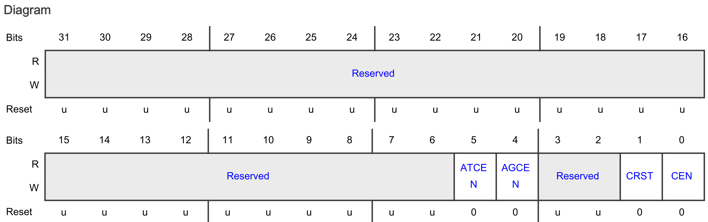
According to the convention, the following defines are available for the CEN bit field in this TCR register:
#define CTIMER_TCR_CEN_MASK   (0x1U)
#define CTIMER_TCR_CEN_SHIFT  (0U)
#define CTIMER_TCR_CEN(x)     (((uint32_t)(((uint32_t)(x)) << CTIMER_TCR_CEN_SHIFT)) & CTIMER_TCR_CEN_MASK)
These defines can for example be used as follows.
// Set the CEN bit field in the TCR register in the CTIMER1 module and leave
// all other bits unchanged. Notice that all three instructions have the same
// result!
CTIMER1->TCR |= CTIMER_TCR_CEN(1);
CTIMER1->TCR |= (1 << CTIMER_TCR_CEN_SHIFT);
CTIMER1->TCR |= CTIMER_TCR_CEN_MASK;

// Reset the CEN bit field in the TCR register in the CTIMER1 module and leave
// all other bits unchanged. Notice that all three instructions have the same
// result!
CTIMER1->TCR &= ~(CTIMER_TCR_CEN(1));
CTIMER1->TCR &= ~(1 << CTIMER_TCR_CEN_SHIFT);
CTIMER1->TCR &= ~(CTIMER_TCR_CEN_MASK);
As a reference, here are several examples for other registers and bits in the MCXA153 microcontroller.
// Set the PCS bit field in the PSR register of LPTMR0 module to 3 and reset
// all others!
LPTMR0->PSR = LPTMR_PSR_PCS(0b11);

// Set the LK bit field in PCR 0 register of PORT3 and reset all other bits!
PORT3->PCR[0] = PORT_PCR_LK(1);

// Check if the TDRE bit field in the STAT register of the LPUART0 module is
// not equal to zero.
if((LPUART0->STAT & LPUART_STAT_TDRE_MASK) != 0)

// Check if the BBF bit field or the MBF bit field in the MSR register of the
// LPI2C module is not equal to zero.
while((LPI2C0->MSR & (LPI2C_MSR_BBF_MASK | LPI2C_MSR_MBF_MASK)) != 0)
Extra
Curious how the three defines for bit field masks evaluate at compile time? Read this!
GPIO output
Resources: ese_driver_examples\gpio\output
Goal
Know how to initialize and control a digital output pin with the GPIO module.
RGB LED - Which pin to use?
The FRDM-MCXA153 board contains an RGB LED that can be controlled by the user. Before being able to control the RGB LED, the physical connection on the FRDM-MCXA153 board must be verified. Checking the board schematic page 7 shows the following pin connections:
- LED_RED: PORT3 pin 12 (P3_12)
- LED_GREEN: PORT3 pin 13 (P3_13)
- LED_BLUE: PORT3 pin 0 (P3_0)
PORTn modules provide support for pin control functions. This microcontroller features four PORT modules: PORT0 to PORT3. Each PORT module is capable of controlling 32 pins (provided that a pin is available on the particular microcontroller package).
Initialization
GPIO modules can be used to control the logic state of a microcontroller pin. However, a pin must first be configured for the GPIO function. This is done in the PORT module. Using P3_13 as an example, it takes the following steps to configure the pin for GPIO:
- Enable the PORT3 and GPIO3 modules in the Module Reset and Clock Control (MRCC) module.
- Initialize P3_13 for GPIO function in the PORT3 module.
- Initialize P3_13 for output function in the GPIO3 module.
These steps are explained in more detail in the following sections.
1. Enable the PORT3 and GPIO3 modules
The MRCC module must be used to enable other modules, such as PORT3 and GPIO3. How this is done is described in the reference manual paragraph 14.3.
// Before a module can be used, its clocks must be enabled (CC != 00) and it
// must be released from reset (MRCC_GLB_RST [peripherals name] = 1). If a
// module is not released from reset (MRCC_GLB_RST [peripherals name] = 0),
// an attempt to access a register within that module is terminated with a
// bus error.
This description translates to the following C instructions for the GPIO3 and PORT3 modules:
// Enable modules and leave others unchanged
// GPIO3: [1] = Peripheral clock is enabled
// PORT3: [1] = Peripheral clock is enabled
MRCC0->MRCC_GLB_CC1 |= MRCC_MRCC_GLB_CC1_GPIO3(1);
MRCC0->MRCC_GLB_CC1 |= MRCC_MRCC_GLB_CC1_PORT3(1);

// Release modules from reset and leave others unchanged
// GPIO3: [1] = Peripheral is released from reset
// PORT3: [1] = Peripheral is released from reset
MRCC0->MRCC_GLB_RST1 |= MRCC_MRCC_GLB_RST1_GPIO3(1);
MRCC0->MRCC_GLB_RST1 |= MRCC_MRCC_GLB_RST1_PORT3(1);
The use of defines such as MRCC_MRCC_GLB_CC1_PORT3(1) for bit fields makes the code very readable and portable. The naming convention for such defines is as follows:
MODULE_REGISTER_BITFIELD(x)
Want to know how this define works and what other defines are available? Read this!
These instructions set bit 0 and bit 8, because according the MRCC_GLB_CC1 and MRCC_GLB_RST register diagrams:
- PORT3 is bit position 0
- GPIO3 is bit position 8
So, alternatively, the following instructions could have been used:
// Enable modules and leave others unchanged
// GPIO3: [1] = Peripheral clock is enabled
// PORT3: [1] = Peripheral clock is enabled
MRCC0->MRCC_GLB_CC1 |= (1<<0);
MRCC0->MRCC_GLB_CC1 |= (1<<8);

// Release modules from reset and leave others unchanged
// GPIO3: [1] = Peripheral is released from reset
// PORT3: [1] = Peripheral is released from reset
MRCC0->MRCC_GLB_RST1 |= (1<<0);
MRCC0->MRCC_GLB_RST1 |= (1<<8);
2. Initialize P3_13 for GPIO function
The PORT module must be used to configure the function for a pin. How this is done is described in the reference manual paragraph 11.4.
// 1. Initialize the pin functions:
//    -  Initialize single pin functions by writing appropriate values to
//       PCRn
//    -  Initialize multiple pins (up to 16) with the same configuration by
//       writing appropriate values to Global Pin Control Low (GPCLR) or
//       Global Pin Control High (GPCHR).
// 2. Lock the configuration for a given pin, by writing 1 to PCRn [LK], so
//    that it cannot be changed until the next reset.
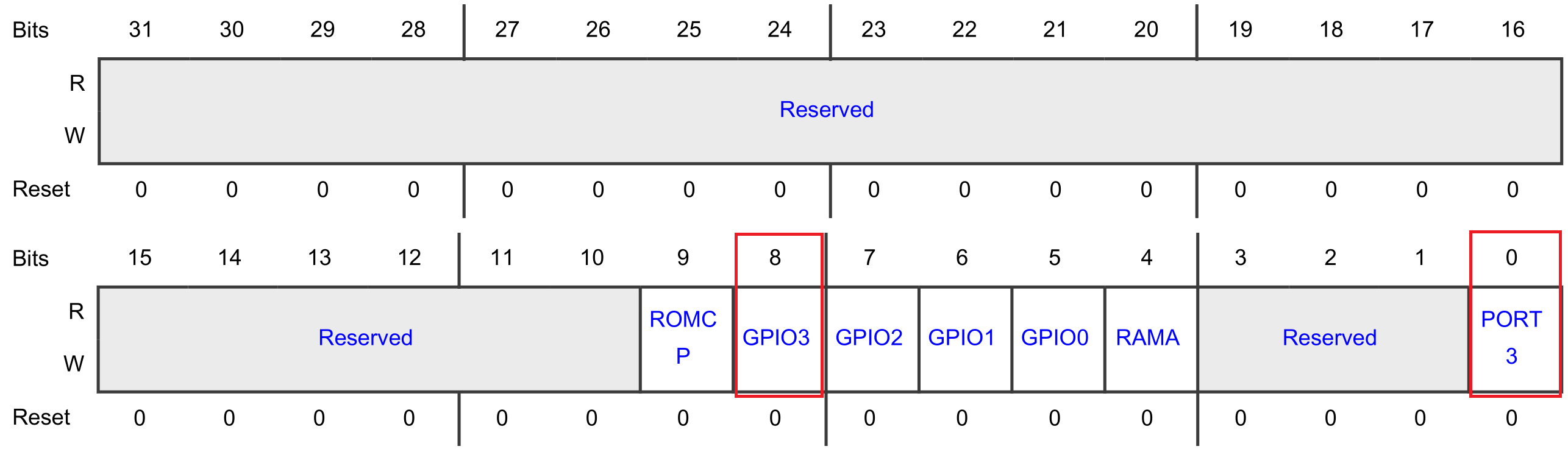
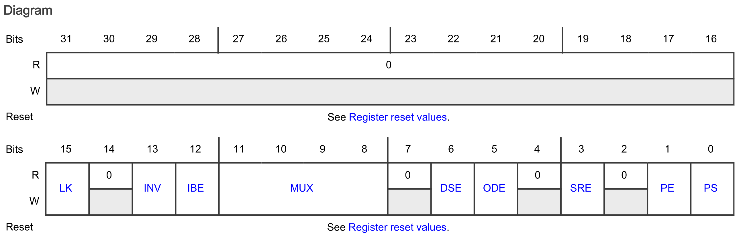
There is a PCR register for each and every pin. The reference manual describes the PCR registers in detail, for example PCR10-PCR13:
Each PORT contains up to 32 PCR registers. These registers all have the same layout, and are organized in an array. The PCR register for P3_13 is addressed as follows:
PORT3->PCR[13]
This register is used as follows for pin P3_13 to:
- Set the LK bit field to [1]: Lock this PCR
-
Set the MUX bit field to [0000]: alternative 0 (GPIO)
Refer to the reference manual paragraph 11.6, find Pin control a (PCR10 - PCR13), find the MUX bit-field description and make sure to understand why the alternative is set to 0 for GPIO.
-
Set all other bit fields to their reset value logic 0
// 1. & 2.
//
// Configure P3_13
// LK : [1] = Locks this PCR
// INV: [0] = Does not invert
// IBE: [0] = Disables
// MUX: [0000] = Alternative 0 (GPIO)
// DSE: [0] = low drive strength is configured on the corresponding pin,
//            if the pin is configured as a digital output
// ODE: [0] = Disables
// SRE: [0] = Fast
// PE:  [0] = Disables
// PS:  [0] = n.a.
PORT3->PCR[13] = 0x00008000;
3. Initialize P3_13 for output function
Refer to the reference manual paragraph 12.5. The following description is provided to initialize a pin for the output function:
// 1. Initialize the GPIO pins for the output function:
//    a. Configure the output logic value for each pin by using Port Data
//       Output (PDOR).
//    b. Configure the direction for each pin by using Port Data Direction
//       (PDDR).
// 2. Interrupt function not used.
Note: The interrupt function is not used in this example.
This description tells that there is a PDOR and PDDR register for the GPIO pins. For P3_13, these registers are addressed as follows:
GPIO3->PDOR
GPIO3->PDDR
Manipulating the 13th bit in these registers, manipulates pin P3_13. The following C instructions can be used, according to the description, to initialize P3_13 as an output pin:
// 1. a.
//
// PDO13: [1] = Logic level 1 – LED green off
GPIO3->PDOR |= (1<<13);

// 1. b.
//
// PDD13: [1] = Output
GPIO3->PDDR |= (1<<13);
Pin toggling
After initialization the pin can be toggled by using the PDOR register in the GPIO peripheral. Setting a bit in the PDOR can also be done by using the PSOR register. For resetting a bit in the PDOR register, the PCOR register can be used.
The following while-loop uses the PSOR and PCOR registers to create a blinking green LED:
while(1)
{
    // LED green off
    // Write logic 1 to bit 13 in the GPIO3 PSOR register so the
    // corresponding bit in PDOR becomes 1
    GPIO3->PSOR = (1<<13);

    // Delay
    for(volatile int i=0; i<1000000; i++)
    {}

    // LED green on
    // Write logic 1 to bit 13 in the GPIO3 PCOR register so the
    // corresponding bit in PDOR becomes 0
    GPIO3->PCOR = (1<<13);

    // Delay
    for(volatile int i=0; i<1000000; i++)
    {}
}
As mentioned, the same blinking functionality could have been achieved by using the PDOR register of PORT3. For example:
// Write logic 1 to PDOR bit 13
GPIO3->PDOR |= (1<<13);

// Write logic 0 to PDOR bit 13
GPIO3->PDOR &= ~(1<<13);
By using the PSOR and PCOR registers, there is no need to read the content of the PDOR register for updating a single bit. If the bitwise operators are used, there are three actions involved: Read-Modify-Write. Hence, this is not not an atomic action, and can thus be interrupted. Writing to the PSOR or PCOR register is an atomic action.
Another alternative for toggling a pin is by using the PTOR register. For example:
// Toggle the pin
GPIO3->PTOR = (1<<13);
Assignment
- Update the application so the red RGB LED blinks, instead of the green RGB LED.
- Update the application and initialize all the pins connected to the RGB LED as GPIO output.
- Update the while-loop to show the following sequence:
red -> green -> blue -> off -> red -> green -> blue -> off -> etc.
Extra
Create an LED chaser.
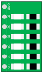
- Use a six LED breakout board, such as
Alternatively, use six LEDs with suitable series resistors. Make sure the anode of the LED is connected to the microcontroller pin and the cathode to GND. Do not forget to add the series resistors.
- Connect the LEDs and the FRDM-MCXA153 board as follows:
| FRDM-MCXA153 | LED |
|---|---|
| GND | GND |
| P2_12 | D1 |
| P2_16 | D2 |
| P2_13 | D3 |
| P2_6 | D4 |
| P3_14 | D5 |
| P3_15 | D6 |
- In the file gpio_output.c correctly configure the pins so they can be used as GPIO output pins. Notice that PORT2 is also used.
TIP: There are two registers for MRCC_GLB_CC: MRCC_GLB_CC0 and MRCC_GLB_CC1. The same applies to MRCC_GLB_RST: MRCC_GLB_RST0 and MRCC_GLB_RST1. Refer to the reference manual to locate these registers and carefully verify where each module (PORT2, GPIO2, PORT3, and GPIO3) is enabled.
- After successfully configuring the pins, create an LED chaser in
main.c.
TIP: So far, delays have been created by for-loops. If you are curious about how to use a timer for that, you might want to take a look at the SysTick timer example. You can also import this example in the IDE from ese_driver_examples\systick\match_interrupt.
GPIO Input - polling
Resources: ese_driver_examples\gpio\input_polling
Goal
Know how to initialize and read a digital input pin by polling a bit in the GPIO module.
Switches - Which pin to use?
The FRDM-MCXA153 board contains three switches. One of these switches is SW3, which is used in this example. However, before being able to read the logic state of SW3, the physical connection on the FRDM-MCXA153 board must be verified. Referring to the board schematic page 7, it shows that PORT1 pin 7 (P1_7) is connected to switch SW3 (a.k.a. WAKEUP).
The schematic also shows that an external pullup resistor is connected to SW3. So, pressing SW3 connects it to GND, reading logic 0.
Initialization
Similar to GPIO output pins, the GPIO modules must be used to read the logic state of a microcontroller pin. However, a pin must first be configured for the GPIO function. Using P1_7 as an example, it takes the following steps to configure the pin for GPIO:
- Enable the PORT1 and GPIO1 modules in the MRCC module.
- Initialize P1_7 for GPIO function in the PORT1 module.
These steps are explained in more detail in the following sections. No additional action is needed, because the default direction of a pin is input.
1. Enable the PORT1 and GPIO1 modules
The MRCC module must be used to enable other modules, such as PORT1 and GPIO1. How this is done is described in the reference manual paragraph 14.3.
// Before a module can be used, its clocks must be enabled (CC != 00) and it
// must be released from reset (MRCC_GLB_RST [peripherals name] = 1). If a
// module is not released from reset (MRCC_GLB_RST [peripherals name] = 0),
// an attempt to access a register within that module is terminated with a
// bus error.
This description translates to the following C instructions:
// Enable modules and leave others unchanged
// PORT1: [1] = Peripheral clock is enabled
// GPIO1: [1] = Peripheral clock is enabled
MRCC0->MRCC_GLB_CC0_SET = MRCC_MRCC_GLB_CC0_PORT1(1);
MRCC0->MRCC_GLB_CC1_SET = MRCC_MRCC_GLB_CC1_GPIO1(1);

// Release modules from reset and leave others unchanged
// PORT1: [1] = Peripheral is released from reset
// GPIO1: [1] = Peripheral is released from reset
MRCC0->MRCC_GLB_RST0_SET = MRCC_MRCC_GLB_RST0_PORT1(1);
MRCC0->MRCC_GLB_RST1_SET = MRCC_MRCC_GLB_RST1_GPIO1(1);
2. Initialize P1_7 for GPIO function
The PORT module must be used to configure the function for a pin. How this is done is described in the reference manual paragraph 11.4.
// 1. Initialize the pin functions:
//    -  Initialize single pin functions by writing appropriate values to
//       PCRn
//    -  Initialize multiple pins (up to 16) with the same configuration by
//       writing appropriate values to Global Pin Control Low (GPCLR) or
//       Global Pin Control High (GPCHR).
// 2. Lock the configuration for a given pin, by writing 1 to PCRn [LK], so
//    that it cannot be changed until the next reset.
There is a PCR register for each and every pin. The reference manual describes the PCR registers in detail. The PCR register for P1_7 is addressed as follows:
PORT1->PCR[7]
This register is used as follows for pin P1_7 to:
- Set the LK bit field to [1]: Lock this PCR.
- Set the IBE bit field to [1]: Input Buffer Enable.
- Set the MUX bit field to [0000]: alternative 0 (GPIO).
- Set all other bit fields to their reset value logic 0.
// 1. & 2.
//
// Configure pins
// LK : [1] = Locks this PCR
// INV: [0] = Does not invert
// IBE: [1] = Digital Input Buffer Enable, otherwise pin is used for analog
//            functions
// MUX: [0000] = Alternative 0 (GPIO)
// DSE: [0] = low drive strength is configured on the corresponding pin,
//            if the pin is configured as a digital output
// ODE: [0] = Disables
// SRE: [0] = Fast
// PE:  [0] = Disables
// PS:  [0] = n.a.
PORT1->PCR[7] = PORT_PCR_LK(1) | PORT_PCR_IBE(1) | PORT_PCR_MUX(0);
Reading the pin logic state
After initialization the pin logic state can be read from PDIR register in the GPIO peripheral. For example:
while(1)
{
    // SW3 pressed?
    if((GPIO1->PDIR & (1<<7)) == 0)
    {
        // Green LED on
        GPIO3->PCOR = (1<<13);
    }
    else
    {
        // Green LED off
        GPIO3->PSOR = (1<<13);
    }
}
Suppose the value of the GPIO1->PDIR register is 0x034045A6 and the if-statement is executed. The question is: Will the green LED be on or off?
The answer to this questions depends on the value of the register (which in turn depends on the connected hardware) and the mask.

The result of the bitwise-and operator is not equal to zero, so the expression in the if-statement is false. The green LED will be off.
Assignment
- Also initialize the pin connected to SW2 as GPIO input pin.
- Update main as follows:
- If SW3 is pressed the green LED switches on
- If SW2 is pressed the green LED switches off
Core clock
Resources: none
The core clock runs by default at 48 MHz.
Goal
Know why the default core clock frequency of the MCXA153 is 48 MHz.
Required hardware
- None
Clocking
So far, the following for-loop has been used to create a delay:
// Delay
for(volatile int i=0; i<1000000; i++)
{}
This gave a nice visual effect, because the blinking of the LED was not too slow nor too fast. A more precise timing, however, is preferred, so let's first find out at which frequency the MCXA153 microcontroller is executing instructions.
The clocking options are depicted in the following figure in chapter 21 of the reference manual.
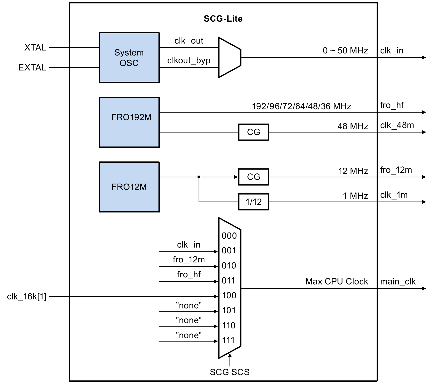
It shows that:
- There is a clocking module called System OSC. OSC means OSCillator. This module derives a clock frequency from an externally connect XTAL oscillator. XTAL means crystal.
- There are two internal clocking modules, called FRO192M and FRO12M. FRO means Free Running Oscillator. M means MHz.
- CG means Clock Gating. This is a means to disable clock signals in order to save power. CG is enabled/disabled by writing bits in specific registers.
- The main_clk can be selected from eight inputs, however, only four are implemented. The main_clk is selected in the SCG module by the SCS bits (located in the CSR register).
The default value (after a reset) of the SCS bits in the SCG->CSR register is described in chapter 22 of the reference manual. The value of these bits is 0b011, which means the option FIRC is selected.
SCS: Returns the currently configured clock source generating the system clock.

000b - Reserved
001b - SOSC
010b - SIRC
011b - FIRC
100b - ROSC
101b-111b - Reserved
And furthermore, referring to section 22.1.3 Clock decoder ring, it shows how the clock name sources in the SCG chapter translate to names throughout the rest of the reference manual:
| SCG chapter name | Reference manual name |
|---|---|
| SOSC | clk_in |
| SIRC | fro_12m |
| FIRC | fro_hf |
| ROSC | clk_16k[1] |
So by default, the fro_hf clock is selected for the main_clk. However, the image shows that this can be one of the following frequencies: 192/96/72/64/48/36 MHz. Paragraph 21.2 states that the fro_hf default frequency is 48 MHz.
Finally, the main_clk is used to clock the CPU and rest of the system. The CPU Clock Divider, as shown in the following figure in chapter 21 of the reference manual, divides this clock. It shows that the AHBCLKDIV register is used to set the divider value.
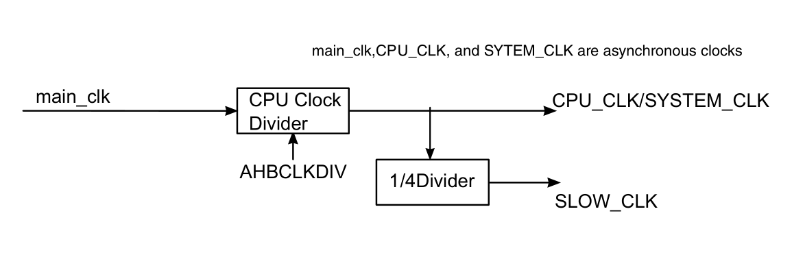
The AHBCLKDIV register in chapter 14 of the reference manual shows that the default (reset) value of the DIV bits:
Clock divider value = (DIV + 1) = 0b00000000 + 1 = 1
So by default, the main_clk is divided by 1.
Conclusion
By default the CPU core clock runs at 48 MHz.
Or is it? Please be aware of the fact that the clock signal generated by the FRO modules have a deviation margin. This margin is specified in the datasheet. In timing critical applications, this deviation might be a problem. In such applications, an external oscillator with better precision can be connected to the XTAL and EXTAL pins.
NVIC
Resources: none
Goal
To understand how the NVIC handles interrupts and use CMSIS to configure the NVIC.
Required hardware
- None
Introduction
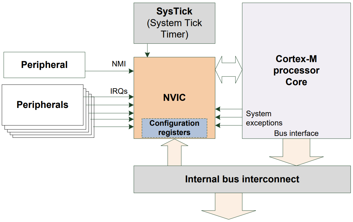
The Nested Vectored Interrupt Controller (NVIC) handles the priority management and masking of interrupts and exceptions. The NVIC is closely coupled with the core as depicted and described in this white paper:
Each interrupt can be in one of the following states:
- Inactive
The interrupt is not active and not pending
- Active
Indicates that this interrupt is being serviced
- Pending
Indicates that an interrupt is waiting to be serviced.
- Active and pending at the same time
The interrupt is being serviced by the core and there is a pending exception from the same source
Nesting
The N in NVIC stands for nested. Nested in the context of microcontrollers means that the handling of one interrupt service handler can be interrupted by another interrupt. For example:

Interrupting another interrupt handler is only possible if the latter interrupt has higher priority. The reference manual section 3.3 describes that the MCXA153 supports 8 interrupt priority levels. These 8 levels are recorded in three bits. For the first four IRQ numbers, this is recorded in Interrupt Priority Register 0 (IPR0) as follows:
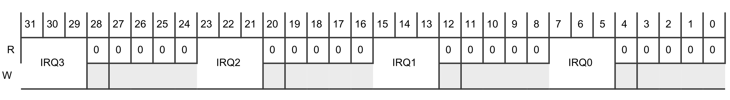
As can be seen in the image, each priority level is recorded in the MSB three bits of a byte. This results in the following priority levels in binary and decimal notation:
0b 000 00000 : 0    -> highest priority
0b 001 00000 : 32
0b 010 00000 : 64
0b 011 00000 : 96
0b 100 00000 : 128
0b 101 00000 : 160
0b 110 00000 : 192
0b 111 00000 : 224  -> lowest priority
Vector
The V in NVIC stands for vectored. Vectored in the context of microcontrollers means that the addresses of the interrupt handlers are stored in a table. In other words, this table stores function pointers (a.k.a. vectors) to the interrupt handlers. As soon as an interrupt is triggered, the microcontroller finds the corresponding address in this table and starts executing the interrupt handler.
The index of an address in this table is also know as the interrupt number (IRQn). The implementation of the entire vector table for the MCXA153 is given in the reference manual in an appendix. An example of a (partial) vector table from one of the example projects is as follows:
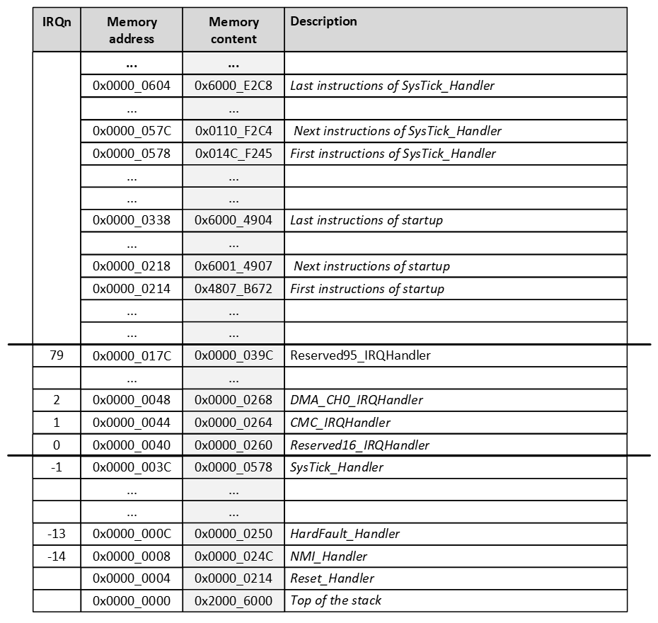
The reference manual contains an appendix called NVIC_configuration.xlsx. In this document the IRQn (NVIC Interrupt ID) of all modules is given. For example, for the GPIO1 module: IRQn=72
The vector table is created by the linker and (normally) stored at the beginning of the flash memory. This is achieved in the examples in the startup file. This startup file uses placeholder names for all interrupt handlers. These are declared with the weak symbol, to denote that if the programmer doesn't provide an interrupt handler, the placeholder implementation should be used.
Special cases of interrupt priority
The NVIC will handle special priority cases as follows:
- New interrupt requested while an interrupt handler is executing?
- New priority higher than current priority?
- New interrupt handler pre-empts current interrupt handler
- New priority lower than or equal to current priority?
- New interrupt held in pending state
- Current handler continues and completes execution
- Previous priority level restored
- New interrupt handled if priority level allows
- New priority higher than current priority?
- Simultaneous interrupt requests and the same priority?
- Lowest interrupt IRQn is serviced first
CMSIS
The NVIC can be read and written by using its registers, similar to all other modules in the microcontroller. However, the NVIC is a module that is available in all Cortex-M microcontrollers. For that reason the CMSIS provides functions to access the NVIC.
Some functions that are often used are:
// Enable a device specific interrupt.
void NVIC_EnableIRQ(IRQn_Type IRQn);

// Set the priority for an interrupt.
void NVIC_SetPriority(IRQn_Type IRQn, uint32_t priority);

// Clear a device specific interrupt from pending.
void NVIC_ClearPendingIRQ(IRQn_Type IRQn);

// Globally enables interrupts.
void __enable_irq();

// Globally disables interrupts.
void __disable_irq();
Microcontroller vendors offer an enumerated type for the IRQn's. So instead of writing
void NVIC_EnableIRQ(31);
for enabling LPUART0 interrupts, the following can be used:
void NVIC_EnableIRQ(LPUART0_IRQn);
Setting the priority of an IRQn can be done in two ways:
- Directly by writing to the IPRn registers.
- By using the CMSIS function NVIC_SetPriority().
There is a difference, because the the CMSIS function assumes a priority value from 0 to 7. Whereas the IPRn registers should have a value as mentioned above. In other words, the following instructions have the same result:
NVIC_SetPriority(GPIO1_IRQn, 3);

NVIC->IPR[GPIO1_IRQn] = 96;
Invalid priority - extra
What happens if (by mistake) the following instruction is executed?
NVIC_SetPriority(GPIO1_IRQn, 96);
What happens next, depends on the implementation of the NVIC_SetPriority() function (see the file CMSIS/Core/Include/core_cm33.h included in all projects):
/**
  \brief   Set Interrupt Priority
  \details Sets the priority of a device specific interrupt or a processor exception.
           The interrupt number can be positive to specify a device specific interrupt,
           or negative to specify a processor exception.
  \param [in]      IRQn  Interrupt number.
  \param [in]  priority  Priority to set.
  \note    The priority cannot be set for every processor exception.
 */
__STATIC_INLINE void __NVIC_SetPriority(IRQn_Type IRQn, uint32_t priority)
{
  if ((int32_t)(IRQn) >= 0)
  {
    NVIC->IPR[((uint32_t)IRQn)]
      = (uint8_t)((priority << (8U - __NVIC_PRIO_BITS)) & (uint32_t)0xFFUL);
  }
  else
  {
    SCB->SHPR[(((uint32_t)IRQn) & 0xFUL)-4UL]
      = (uint8_t)((priority << (8U - __NVIC_PRIO_BITS)) & (uint32_t)0xFFUL);
  }
}
For the MCXA153, __NVIC_PRIO_BITS is defined as 3. This means the provided priority will be bitwise left shifted 8 - 3 = 5 positions. With a value of 96 (=0b01100000), this means: (0b01100000 << 5) = 0b00000000.
The result is that the priority will be set to 0, which is the highest priority.
ISR considerations
When writing ISR's it is considered good practice to:
- Clear an interrupt in both the NVIC and module.
- Keep code as short as possible in the ISR.
- Declare global variables volatile that are used in the ISR to prevent the compiler from optimization.
GPIO input - interrupt
Resources: ese_driver_examples\gpio\input_interrupt
Goal
Know how to initialize and read a digital input pin by using interrupts in the GPIO module.
Initialization
It takes the following steps to configure P1_7 (SW3) for GPIO:
- Enable the PORT1 and GPIO1 modules in the MRCC module.
-
Initialize P1_7 for GPIO function in the PORT1 module.
No additional action is needed, because the default direction of P1_7 is input. These steps are exactly the same when compared to the polling example.
Using interrupts on a GPIO input pin requires two additional steps:
-
Enable the desired interrupt in the GPIO module.
- Enable GPIO1 interrupts in the NVIC module.
These steps are explained in more detail in the following sections.
1. Enable the PORT1 and GPIO1 modules
// Enable modules and leave others unchanged
// PORT1: [1] = Peripheral clock is enabled
// GPIO1: [1] = Peripheral clock is enabled
MRCC0->MRCC_GLB_CC0_SET = MRCC_MRCC_GLB_CC0_PORT1(1);
MRCC0->MRCC_GLB_CC1_SET = MRCC_MRCC_GLB_CC1_GPIO1(1);

// Release modules from reset and leave others unchanged
// PORT1: [1] = Peripheral is released from reset
// GPIO1: [1] = Peripheral is released from reset
MRCC0->MRCC_GLB_RST0_SET = MRCC_MRCC_GLB_RST0_PORT1(1);
MRCC0->MRCC_GLB_RST1_SET = MRCC_MRCC_GLB_RST1_GPIO1(1);
2. Initialize P1_7 for GPIO function
// Configure pin P1_7
// LK : [1] = Locks this PCR
// INV: [0] = Does not invert
// IBE: [1] = Digital Input Buffer Enable, otherwise pin is used for analog
//            functions
// MUX: [0000] = Alternative 0 (GPIO)
// DSE: [0] = low drive strength is configured on the corresponding pin,
//            if the pin is configured as a digital output
// ODE: [0] = Disables
// SRE: [0] = Fast
// PE:  [0] = Disables
// PS:  [0] = n.a.
PORT1->PCR[7] = PORT_PCR_LK(1) | PORT_PCR_IBE(1) | PORT_PCR_MUX(0);
3. Enable the desired interrupt in the GPIO module.
The GPIO module has an Interrupt Control Register (ICR) for each pin. These registers are organized in an array, so the ICR register for P1_7 is used as follows:
GPIO1->ICR[7]
This register contains two bit fields as can be seen in the reference manual.
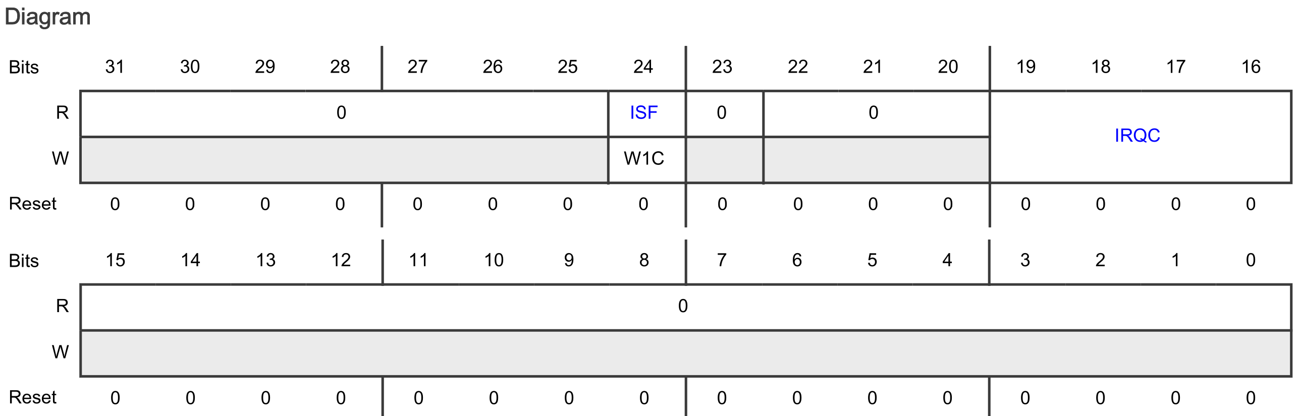
The bit fields are:
- ISF
- Means: Interrupt Status Flag
- Indicates whether the configured interrupt is detected. The pin interrupt configuration is valid in all digital pin muxing modes.
- The ISF bit field shows the text W1C. W1C means Write 1 to clear (w1c). See reference manual paragraph 1.5.4.
- The Interrupt Status Flag Register 0 (ISFR0) can also be used to check the interrupt status of P1_7. See reference manual paragraph 12.7.1.15
- IRQC
- The IRQC bit field contains 4 bits, giving a total of 16 ISF and DMA request configuration options.
- Out of reset, the IRQC bit field is 0b0000. Checking the IRQC configuration
- description in the reference manual: 0000b means that ISF is disabled.
Configuring P1_7 for setting the ISF and generating an interrupt on falling edges is done as follows:
// ISF: [1] = Clear the flag
// IRQC : [1010] = ISF and interrupt on falling edge
GPIO1->ICR[7] = GPIO_ICR_ISF(1) | GPIO_ICR_IRQC(0b1010);
4. Enable GPIO1 interrupts in the NVIC module.
Enabling interrupts for GPIO1 in the NVIC:
// Enable GPIO1 interrupts
NVIC_SetPriority(GPIO1_IRQn, 3);
NVIC_ClearPendingIRQ(GPIO1_IRQn);
NVIC_EnableIRQ(GPIO1_IRQn);
Interrupt handler
The interrupt handler for GPIO handles the interrupt request. The following must be done:
- Clear the interrupt in the NVIC.
- The same interrupt handler is executed for all GPIO1 pins. Check to make sure the interrupt was triggered by P1_7 (although strictly speaking, this is not necessary in this example as there is only one pin generating an interrupt).
- Clear the interrupt in the GPIO module.
- Handle the event.
The result is as follows:
void GPIO1_IRQHandler(void)
{
    // Clear the interrupt
    NVIC_ClearPendingIRQ(GPIO1_IRQn);

    // Interrupt handler triggered by P1_7?
    if((GPIO1->ISFR[0] & GPIO_ISFR_ISF7(1)) != 0)
    {
        // Clear the flag
        GPIO1->ISFR[0] = GPIO_ISFR_ISF7(1);

        // Handle the event
        cnt++;
    }
}
Note the use of a global variable called cnt. This variable is incremented on every interrupt generation. This is a global variable declared as follows:
static volatile uint32_t cnt = 0;
This variable is declared static, because the scope is limited to this file.
This variable is declared volatile, because the variable can change outside normal program flow (because it is used in an ISR). The compiler should not optimize any read/write operations.
Assignment
Change this example so it uses SW2 and the blue RGB LED.
Some tips:
- Find the pin that is connected to SW2 in the board schematic.
- Another GPIO module also requires another interrupt handler.
Assignment - Rotary encoder
Resources: ese_shieldv3_examples\encoder\gpio
Goal
To practice with the modules discussed so far.
Hardware requirements
- FRDM-MCXA153 board
- Rotary encoder, such as available on Shield V3 or Mikroe-1824 add-on board
- Type-C USB cable
Note. When using the Mikroe add-on board, different pins must be used!
Functional requirements
The application uses the RGB LED and a rotary encoder. It must implement the following functional requirements.
-
The application keeps track of the number of CW and CCW pulses.
a. pulses = 0: RGB LEDs off.
b. pulses > 0: Green LED on; Red LED off.
c. pulses < 0: Green LED off; Red LED on.
-
A CW pulse increments the number of pulses by 1.
- A CCW pulse decrements the number of pulses by 1.
- Pressing the encoder switch resets the pulses to 0.
- After a microcontroller reset, pulses is reset to 0.
Architecture
The Shield V3 shows an example of how to connect the hardware parts.
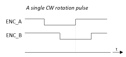
The ENC_A and ENC_B signals encode the rotation direction. An example timing diagram for a single clockwise (CW) rotation pulse:
And an example timing diagram for a single counter clockwise (CCW) rotation pulse:
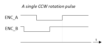
Notice from both timing diagrams that on a rising edge of ENC_A, the sampled logic value of ENC_B is different for CW and for CCW rotations.
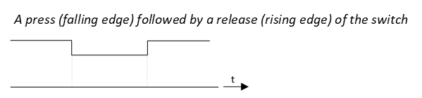
The ENC_SW signal reflects the logic state of the encoder switch as follows:
API
In order to create the functional requirements, the following API functions are prepared.
/*!
 * \brief Initializes the RGB LED pins
 *
 * - Red LED   | P3_12 | GPIO output
 * - Green LED | P3_13 | GPIO output
 * - Blue LED  | P3_0  | GPIO output
 */
void gpio_output_init(void);
/*!
 * \brief Initializes the encoder pins
 *
 * - ENC_A  | P3_31 | GPIO input with interrupts enabled on rising edges
 * - ENC_B  | P2_7  | GPIO input
 * - ENC_SW | P1_6  | GPIO input with interrupts enabled on both edges
 */
void encoder_init(void);
/*!
 * \brief Resets the counted pulses.
 *
 * Resets the internal pulses counter to 0.
 */
void encoder_reset(void);
/*!
 * \brief Returns the number of pulses in CW or CCW direction since last reset
 *
 * The function keeps track of the CW and CCW pulses. For every CW pulse, an
 * internal counter is incremented. For every CCW pulse, that same counter is
 * decremented.
 *
 * Meaning:
 *   - If the function returns 0, no pulses were counted or as much CW pulses as
 *     CCW pulses
 *   - If the function returns a value < 0, that much more number of CCW pulses
 *     were detected.
 *   - If the function returns a value > 0, that much more number of CW pulses
 *     were detected.
 *
 * \return The number of pulses counted since last reset
 */
int32_t encoder_pulses(void);
/*!
 * \brief Detects if the switch was pressed.
 *
 * This firmware driver remembers if the switch was pressed with an internal
 * flag. When this function is called, it resets the internal flag.
 *
 * \return True if the switch was pressed.
 */
bool encoder_sw_pressed(void);
/*!
 * \brief Detects if the switch was released.
 *
 * This firmware driver remembers if the switch was released with an internal
 * flag. When this function is called, it resets the internal flag.
 *
 * \return True if the switch was released.
 */
bool encoder_sw_released(void);
Implementation tips
- Start with the RGB LED GPIO output pins. Verify in main that the RGB works as expected.
For the encoder rotation detection:
- Configure ENC_A and ENC_B pins for GPIO input.
- Configure ENC_A pin to generate interrupts on rising edges.
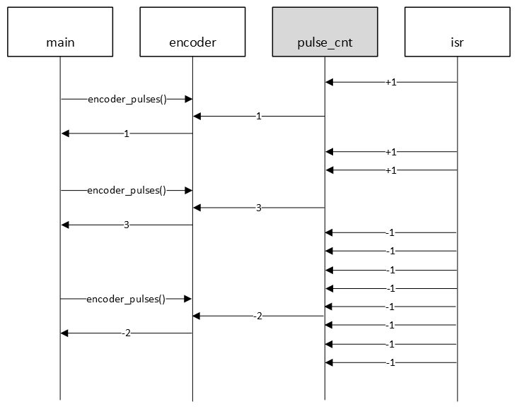
- When such an interrupt occurs, sample the logic input value of the ENC_B pin:
- if ENC_B pin = 0, then CW rotation, so internal counter pulse_cnt + 1
- if ENC_B pin = 1, then CCW rotation, so internal counter pulse_cnt - 1
This behaviour is illustrated in the following sequence diagram.
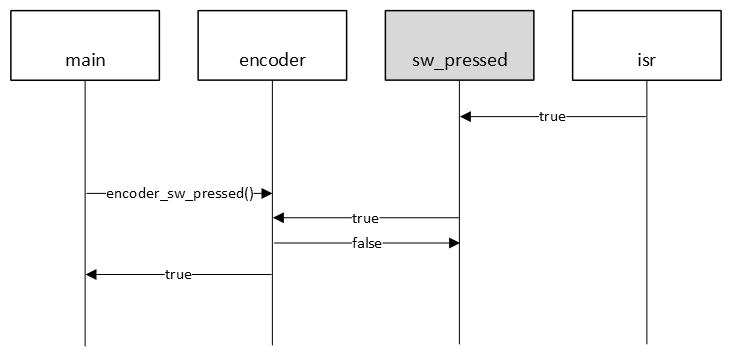
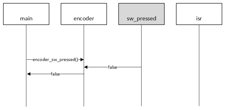
For the encoder switch:
- Configure ENC_SW for GPIO input.
- Configure ENC_SW pin to generate interrupts on falling edges.
- When such an interrupt occurs, set an internal boolean flag sw_pressed indicating a SW press.
The following sequence diagram illustrates this behaviour for when the switch was pressed.
Or, the same example, but now when the switch was not pressed.
Timers - Introduction
Resources: none
Goal
To understand the general operation of timers/counters.
Timers/counter
Generally speaking, timers are binary counters that count up/down in single steps to a top value and will start over again. This principle is depicted in the following block diagram.
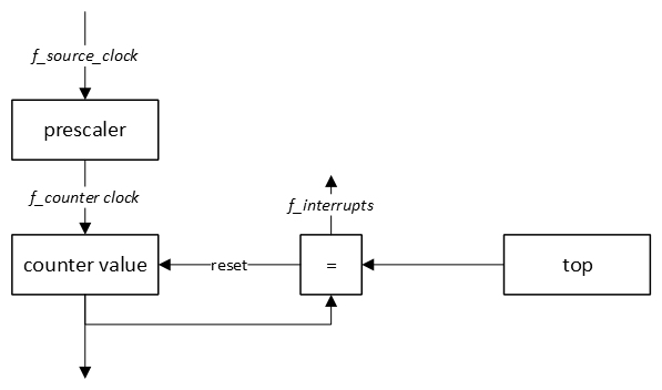
The frequency at which interrupts are generated (f_interrupts) is equal to:
f_interrupts = f_source_clock / prescaler / (top + 1)
Or rewritten to the time between two interrupts (T_interrupts):
T_interrupts = T_source_clock * prescaler * (top + 1)
The number of pulses counted by most timers is equal to (top + 1), because the timer starts counting from 0. This, however, is implementation dependent.
For a timer that counts up, the following general timing diagram is applicable.
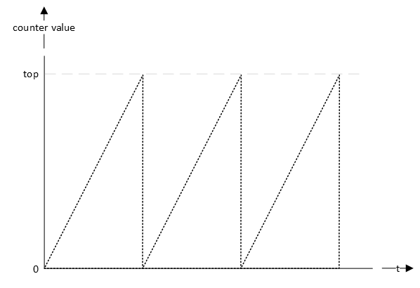
Although this simplified basic representation is applicable for all timers, implementations of timer modules range from very basic to very complex. Timers can be used to capture and/or generate a variety of signals, such as square waves, PWM signals, pulse counting, etc.
SysTick
Resources: ese_driver_examples\systick\match_interrupt
Goal
To know what the SysTick module is and how to use the SysTick module for generating interrupts at a fixed interval.
System Tick Timer
The Cortex-M33 core comes with an integrated timer module, called the System Tick Timer (SysTick). This timer is often used by operating systems (OS), because this very same module is available in all Cortex-M microcontrollers. For applications that do not require an OS, the SysTick can be used for time keeping, time measurement, or as an interrupt source for tasks that need to be executed regularly.
Characteristics of the Cortex-M33 SysTick timer are:
- 24-bit down counter
- Clocked by the CPU_CLK
- The interrupt controller clock updates the SysTick counter. If this clock signal is stopped for low-power mode, the SysTick counter stops.
Accessing the SysTick module
The registers of the SysTick module are memory mapped. Clearing the CTRL register, for example, can be done as follows:
SysTick->CTRL = 0;
However, CMSIS provides a universal function to configure the SysTick module for all Cortex-M devices. The function prototype is:
uint32_t SysTick_Config(uint32_t ticks);
Verification of the default CPU clock setting
By default, the CPU is clocked with a frequency of 48 MHz. This means the SysTick timer is also clocked with 48 MHz. If we were to generate an interrupt every second, the CMSIS function would be called as follows:
// Generate an interrupt every 1s. Note that this will not work,
// because 480000000 > 2^24.
SysTick_Config(48000000);
However, 480000000 > 2^24, so this will not fit. The CMSIS function SysTick_Config() checks if the parameter ticks is within the 24-bit range. If not, the SysTick timer will not be started.
Instead of generating interrupts every second, let's generate an interrupt every millisecond. This is one thousand times faster than generating interrupts every second, so the function is called as follows:
// Generate an interrupt every 1ms
SysTick_Config(48000);
In general:
ticks = f_cpu / f_systick_interrupts
Interrupts are disabled by default and can be enabled by using the CMSIS compliant function:
// Enable interrupts
__enable_irq();
In this example, the while-loop is empty. With the Wait For Interrupt (WFI) instruction, the microcontroller can be put into a sleep mode.
while(1)
{
    // Wait for interrupt
    __WFI();
}
Finally, an interrupt handler is required. The CMSIS compliant function name is SysTick_Handler(). This name can also be found in the vector table in the startup file.
void SysTick_Handler(void)
{
    // Toggle the green LED
    GPIO3->PTOR = (1<<13);
}
Verification
Verify that the green LED is on. The frequency is too high for the human eye to see the LED blinking. Connecting a logic analyzer to P3_13 shows:
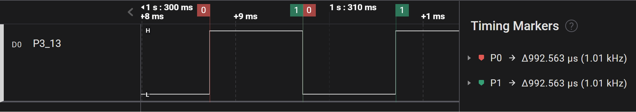
This is very close to the expected 1 ms pulse width.
Assignment
- In main.c, add a global variable called ms as follows:
static volatile uint32_t ms = 0;
- Update the SysTick_Handler() as follows:
void SysTick_Handler(void)
{
    ms++;

    if((ms % 1000) == 0)
    {
        // Toggle the green LED
        GPIO3->PTOR = (1<<13);
    }
}
-
Build and run the application.
Q1Explain the result. -
ms is an 32-bit unsigned variable.
Q2How many days can be recorded if this variable is incremented every millisecond, before it starts from zero again? -
In Arduino, there is a millis() function that returns the number of milliseconds since microcontroller startup. Instead of using a function, we can use the ms variable. In main use the variable to create a blinky without delay. It toggles the red LED every 2 seconds (0.5Hz).
Critical sections
Resources: ese_general_examples\advanced\critical_section
Goal
To know how to protect a data object that requires multiple read or write operations.
Definitions
Before starting the discussion on how to protect a data object, it is good to be familiar with the following definitions:
Race condition
Anomalous behaviour due to unexpected critical dependence on the relative timing of events.
Critical section
A section of code which creates a possible race condition. The code section should only be executed by one process at a time.
Atomic
Indivisible access to any data object. For Cortex-M microcontrollers, the native object size is 32-bits. This means accessing data objects that are 32-bits or smaller takes a single clock cycle. This is indivisible. Data objects larger than 32-bits (such as structs), require more than one instruction to access (both reading and writing) and hence takes more then one clock cycle. This access could thus be interrupted.
Volatile
Directive for the compiler. Indicates that a variable may change outside of the control of some code. For example a module's register. Or a variable updated in an interrupt handler.
Introduction
Accessing data in a microcontroller takes time. For example reading a 32-bit integer variable. Or writing a 16-bit value to a register. The time these actions take depend on the native object size of the microcontroller. For Cortex-M microcontrollers the native object size is 32-bits. Accessing objects of the native size or smaller are atomic.
It is common to work with data objects that are larger than the native object size. A struct is an example. Another example is all objects in an array. It takes more than one instruction to read or write the entire object. As multiple instructions can be interrupted, this might cause a race condition.
Example - no race condition
The following timing diagram shows the interaction between three processes: sw3, main and systick_isr. The main application checks if SW3 is pressed by using the sw3 process. If so, it will read all values from the shared data object global_buffer (in a for-loop) and print them using the LPUART. The systick_isr interrupt handler is executed every 1 second and writes the entire buffer with one and the same value, depending on the number of seconds passed.
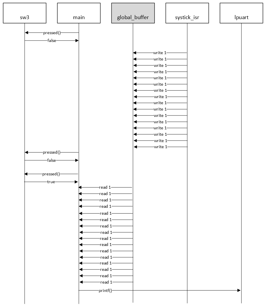
This nice weather scenario produces, for example, the following output:
1111111111111111
3333333333333333
6666666666666666
9999999999999999
1111111111111111
2222222222222222
Example - Race condition
The execution of main depends on the input of the user. If SW3 is clicked within a certain time window, main might have started copying the global_buffer, but it gets interrupted by the systick_isr interrupt handler. This interrupt handler overwrites the entire shared object's content. As soon as the interrupt handler is finished the main continues copying with the updated value. This scenario is depicted in the following timing diagram.
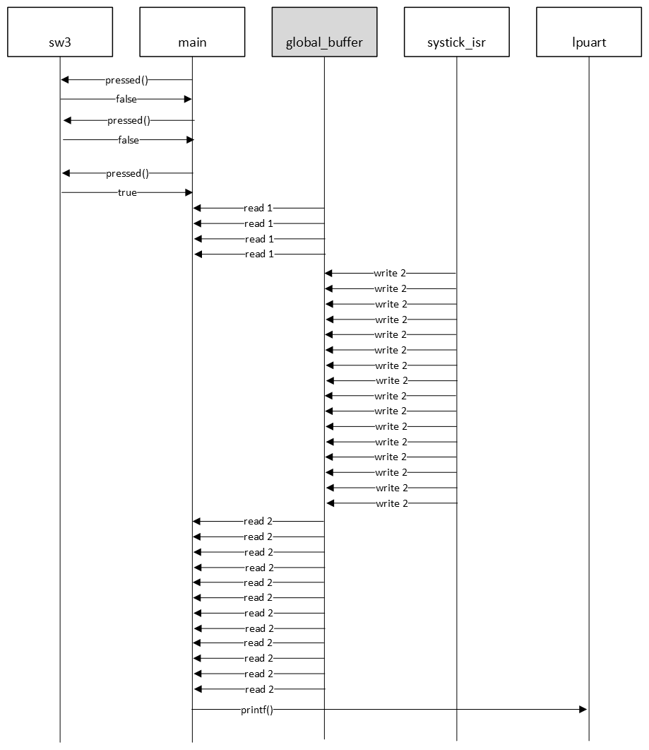
This race condition scenario produces, for example, the following output:
1111111111111111
3333333333333333
6666666666666666
9999999999999999
1111222222222222  <--  Reading the global_buffer got unintentionally interrupted
2222222222222222
In this example, reading the global_buffer in main is the critical section. This section can be protected for pre-emption by globally disabling interrupts. This is done as follows with as few instructions as possible and makes sure that the previous state of the global interrupt setting is restored when the critical section is finished.
// Critical section start
uint32_t m = __get_PRIMASK();
__disable_irq();

// critical section goes here ...

__set_PRIMASK(m);
// Critical section end
The functions used in the code snippet above are part of the CMSIS. These functions are available for all Cortex-M microcontrollers.
Assignment
- Open the VCOM (115200-8n1) in a terminal application of your choice.
- Press SW3. Try to get the timing right and trigger the race condition (the buffer printing different values on a single SW3 click).
In the main-loop, there is an artificial delay. Increase the delay by a factor 10 as follows and try to trigger the race condition again.
// Artificial delay to increase the chance of interrupting this
// critical section
for(uint32_t d=0; d<200000; d++)
{}
Q1 Why does increasing the artificial delay make it easier to trigger the race condition?
Leave the increased delay in the code.
Q2 Protect the critical section from pre-emption by updating the code.
If implemented correctly you should observe two things:
- The printed line is always correct (showing one distinct character).
- Clicking SW3 twice quickly prints one or two characters, pauses for a little bit and then finishes printing.
Q3 Explain observation number 2.
Low-Power Timer
Resources: ese_driver_examples\lptmr\match_interrupt
Goal
To know what the LPTMR module is and how to use the LPTMR module for generating interrupts at a fixed interval.
LPTMR features
The MCXA153 has one instance of the LPTMR module. It is called LPTMR0. The LPTMR is described in the reference manual chapter 34.
Some characteristics of the LPTMR module are:
- 32-bit counter.
- Can be clocked from one of four sources determined by the PCS bit field in the LPTMR0->PSR register.
- The LPTMR allows the maximum clock frequency of 25 MHz.
- In low-power modes, LPTMR continues to operate normally.
LPTMR clocking
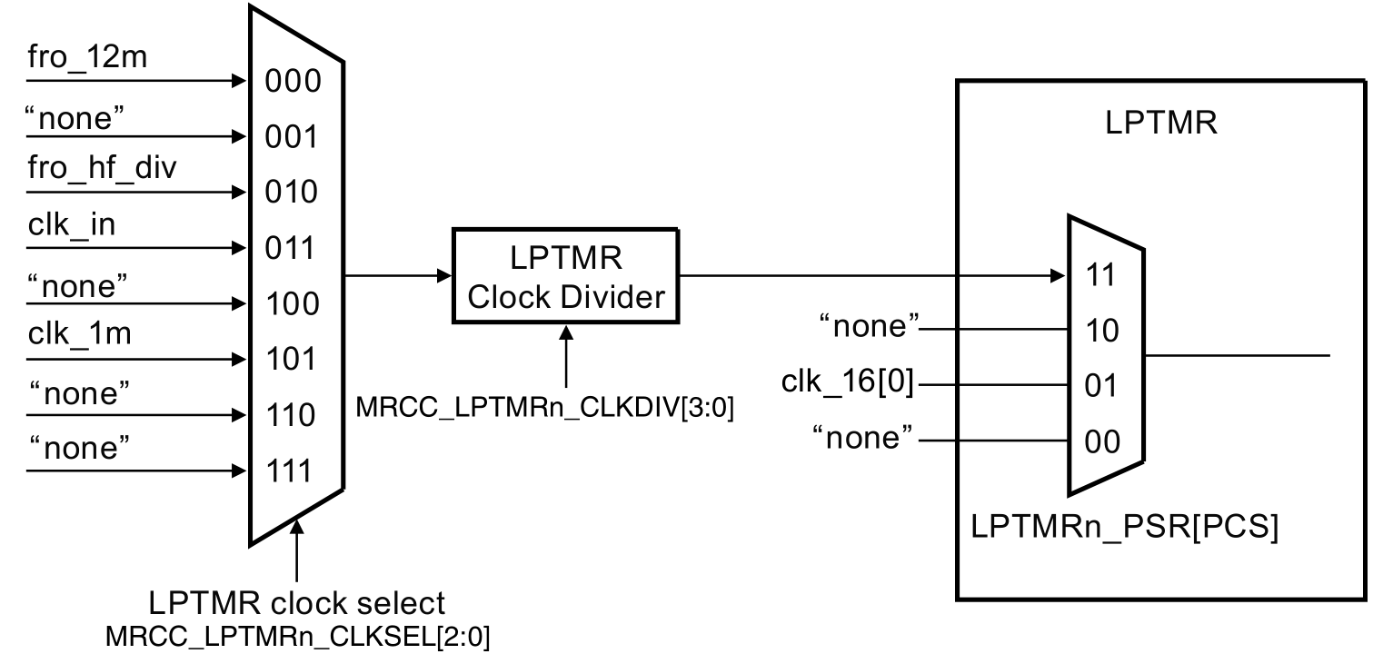
Clocking the LPTMR is established by configuring several bits in registers of the MRCC- and LPTMR module. This is depicted in the following image.
An example
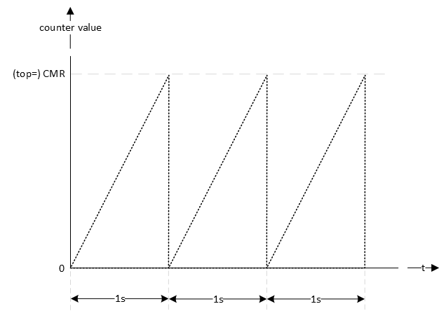
In this example, the LPTMR is configured to generate an interrupt every second. This is depicted in the following timing diagram. CMR is the compare register and when the counter value matches the CMR register, the counter should reset.
First the clock source for the timer should be established. This is application dependent, but let's choose the CLK_1M. Dividing this clock by 1 million generates an interrupt every second. The reference manual chapter 34.5 describes how to initialize LPTMR0.
void lptmr0_init(void)
{
    // Set clock source
    // MUX: [101] = CLK_1M
    MRCC0->MRCC_LPTMR0_CLKSEL = MRCC_MRCC_LPTMR0_CLKSEL_MUX(0b101);

    // Set clock divider
    // HALT: [0] = Divider clock is running
    // RESET: [0] = Divider isn't reset
    // DIV: [0000] = divider value = (DIV+1) = 1
    MRCC0->MRCC_LPTMR0_CLKDIV = 0;

    // From section 34.5 Initialization (NXP, 2024)
    //
    // Perform the following procedure to initialize LPTMR:
    // 1. Configure Control Status (CSR) for the selected mode and pin
    //    configuration, when CSR[TEN] is 0. This resets the counter and clears
    //    the flag.
    // 2. Configure Prescaler and Glitch Filter (PSR) with the selected clock
    //    source and prescaler or glitch filter configuration.
    // 3. Configure Compare (CMR) with the selected compare point.
    // 4. Write 1 to CSR[TEN] to enable LPTMR.

    // 1.
    //
    // - TDRE : [0] = Timer DMA request disable
    // - TCF : [1] = Clears the Timer Compare Flag
    // - TIE : [0] = Timer interrupt disable
    // - TPS : [00] = Timer Pin Select is not used, leave at default value
    // - TPP : [0] = Timer Pin Polarity is not used, leave at default value
    // - TFC : [0] = CNR is reset whenever TCF is set
    // - TMS : [0] = Time Counter mode
    // - TEN : [0] = LPTMR is disabled
    LPTMR0->CSR = LPTMR_CSR_TCF(1);

    // 2.
    //
    // - PRESCALE : [0000] = n.a.
    // - PBYP : [1] = Prescaler and glitch filter disable
    // - PCS : [11] = Clock 3 is Combination of clocks configured in
    //                MRCC_LPTMR0_CLKSEL[MUX] field in SYSCON module. The Clock
    //                frequency must be less than 25 MHz to be used as a clock
    //                for the Low Power Timers.
    LPTMR0->PSR = LPTMR_PSR_PBYP(1) | LPTMR_PSR_PCS(0b11);

    // 3.
    //
    // Generate an interrupt every second
    LPTMR0->CMR = 1000000-1;

    // 4.
    //
    // - TDRE : [0] = Timer DMA request disable
    // - TCF : [1] = Clears the Timer Compare Flag
    // - TIE : [1] = Timer interrupt enable
    // - TPS : [00] = Timer Pin Select is not used, leave at default value
    // - TPP : [0] = Timer Pin Polarity is not used, leave at default value
    // - TFC : [0] = CNR is reset whenever TCF is set
    // - TMS : [0] = Time Counter mode
    // - TEN : [1] = LPTMR is enable
    LPTMR0->CSR = LPTMR_CSR_TCF(1) | LPTMR_CSR_TIE(1) | LPTMR_CSR_TEN(1);

    // Enable Interrupts
    NVIC_SetPriority(LPTMR0_IRQn, 0);
    NVIC_ClearPendingIRQ(LPTMR0_IRQn);
    NVIC_EnableIRQ(LPTMR0_IRQn);
}
The interrupt handler is implemented as follows. The name of the handler is defined in the startup file.
void LPTMR0_IRQHandler(void)
{
    // Clear pending IRQ
    NVIC_ClearPendingIRQ(LPTMR0_IRQn);

    // Clear status flag by writing 1
    LPTMR0->CSR |= LPTMR_CSR_TCF_MASK;

    // Handle the event
    lptmr0_timeout_flag = true;
}
Notice the use of the global variable lptmr0_timeout_flag. This flag can be checked in the main application. The following example checks if the flag is true, set it to false en toggle the green LED.
while(1)
{
    // LPTMR flag true?
    if(lptmr0_timeout_flag == true)
    {
        // Set it false
        lptmr0_timeout_flag = false;

        // Toggle green LED
        GPIO3->PTOR = (1<<13);
    }
}
Assignment
There is more than one way to slow down the generation of interrupts. For example, for generating interrupts with an interval twice as long:
- Set the functional divider to 2, by setting the DIV bit field to 1 in the MRCC0->MRCC_LPTMR0_CLKDIV register.
- Enable and set the prescaler to 2 in the LPTMR0->PSR register.
- Double the value written in the LPTMR0->CMR register.
Implement all of the above. If correct, the green LED toggles approximately every 8 seconds.
Note
Although not used in this example project, reading the LPTMR counter value is different compared to the other timers. This is what is mentioned in the reference manual in section 34.3.5:
You cannot initialize CNR but can read it at any time. On each read of CNR, you must first write a value to it. This synchronizes and registers the current value of CNR into a temporary register. The contents of the temporary register are returned on each read of CNR.
So, reading the counter value is done as follows:
// Reading the CNR value requires that it is written first (see reference manual
// section 34.3.5)
LPTMR0->CNR = 0;
uint32_t cnr_value = LPTMR0->CNR;
Standard Counter or Timer - match
Resources: ese_driver_examples\ctimer\match_interrupt
Goal
Know how to use the standard counter or timer (CTIMER) module to periodically generate interrupts.
Standard Counter or Timer
The MCXA153 microcontroller features three Standard Counter or Timer (CTIMER) modules. Features of each module include:
- 32-bit binary counter
- 32-bit prescaler
- Four 32-bit capture registers to take a snapshot of the binary counter when an input signal transitions
- Four 32-bit match registers
- To control timer operations
- Generate external outputs
- Setup for PWM operation, allowing up to three single-edged controlled PWM outputs
CTIMER clocking
Clocking the CTIMER is depicted in the following image.
CTIMER in match interrupt mode
In this example, CTIMER 1 channel 0 is configured to generate an interrupt every second. This is depicted in the following timing diagram. MAT0 is the compare register and when the counter value matches the MAT0 register, the counter must be reset.
Generating interrupts at a regular interval with a CTIMER can be done by following the initialization steps as described in the reference manual paragraph 26.1.5.
- Select a clock source for the CTIMER using MRCC_CTIMER0_CLKSEL, MRCC_CTIMER1_CLKSEL, and MRCC_CTIMER2_CLKSEL registers.
- Enable the clock to the CTIMER via the CTIMERGLOBALSTARTEN[CTIMER0_CLK_EN], CTIMERGLOBALSTARTEN[CTIMER1_CLK_EN], and CTIMERGLOBALSTARTEN[CTIMER2_CLK_EN] fields. This enables the register interface and the peripheral function clock.
- Clear the CTIMER peripheral reset using the MRCC_GLB_RST0 registers.
- Each CTIMER provides interrupts to the NVIC. See MCR and CCR registers in the CTIMER register section for match and capture events. For interrupt connections, see the attached NVIC spreadsheet.
- Select timer pins and pin modes as needed through the relevant PORT registers.
- The CTIMER DMA request lines are connected to the DMA trigger inputs via the DMAC0_ITRIG_INMUX registers (See Memory map and register definition). Note that timer DMA request outputs are connected to DMA trigger inputs.
As an example, CTIMER1 will be configured to generate interrupts with a frequency of 1 Hz. This doesn't require the use of pins or DMA requests, so steps 5. and 6. can be omitted. The other steps are explained in more detail in the following sections.
1. Select a clock source
The source clock is selected in the MRCC module. From the available options, 1 MHz is selected. Furthermore, the source clock is configured to run and the divider is set to 1. This divider can be seen as an additional prescaler (available in the MRCC module).
// MUX: [101] = CLK_1M
MRCC0->MRCC_CTIMER1_CLKSEL = MRCC_MRCC_CTIMER1_CLKSEL_MUX(0b101);

// HALT: [0] = Divider clock is running
// RESET: [0] = Divider isn't reset
// DIV: [0000] = divider value = (DIV+1) = 1
MRCC0->MRCC_CTIMER1_CLKDIV = 0;
2. Enable the clock to the CTIMER
The CTIMER module interface and function clock are disabled by default. These are enabled in the SYSCON module as follows:
// CTIMER1_CLK_EN: [1] = CTIMER 1 function clock enabled
SYSCON->CTIMERGLOBALSTARTEN |= SYSCON_CTIMERGLOBALSTARTEN_CTIMER1_CLK_EN(1);
3. Clear the CTIMER peripheral reset
Similar to all other modules, the CTIMER needs to be enabled and released from reset in the MRCC module:
// Enable modules and leave others unchanged
// CTIMER1: [1] = Peripheral clock is enabled
MRCC0->MRCC_GLB_CC0_SET = MRCC_MRCC_GLB_CC0_CTIMER1(1);

// Release modules from reset and leave others unchanged
// CTIMER1: [1] = Peripheral is released from reset
MRCC0->MRCC_GLB_RST0_SET = MRCC_MRCC_GLB_RST0_CTIMER1(1);
4. Setup NVIC
In order to generate interrupts at the desired interval of 1 Hz, the prescaler and top value must be configured.
Using the equation from timers introduction:
f_interrupts = f_source_clock / prescaler / (top + 1)
      1Hz    =      1 MHz     / prescaler / (top + 1)
This yields a single equation with two unknowns. However, a value can be chosen for one of the unknowns:
      1Hz    =       1MHz     /   1000    / (top + 1)
      1Hz    =             1 kHz          / (top + 1)
 =>
    (top + 1)= 1 kHz / 1 Hz
    (top + 1)=     1000
Finally, check if both the chosen and calculated value fit within 32-bit registers. This is true, because in both cases 1000 < 2^32.
Each timer has four match channels. For generating a single interrupt, the selected channel doesn't matter, so let's select match register channel 0 (MR0). Three bits need to be configured for MR0:
- MR0S - Stop on MR0 Stops Timer Counter (TC) and Prescale Counter (PC), and turns TCR[CEN] to 0 if MR0 matches Timer Counter (TC). Must be 0, because the timer must keep on running to generate interrupt periodically
- MR0R - Reset on MR0 Resets Timer Counter (TC) if MR0 matches its value. Must be 1, because the timer must restart from zero on a match.
- MR0I - Interrupt on MR0 Generates an interrupt when MR0 matches the value in Timer Counter (TC). Must be 1, because an interrupt must be generated.
// Specifies the prescale value. 1 MHz / 1000 = 1 kHz
CTIMER1->PR = 1000-1;

// Match value for match register 0. 1 kHz / 1000 = 1 Hz
CTIMER1->MR[0] = 1000-1;

// MR0S: [0] = Does not stop Timer Counter (TC) if MR0 matches Timer Counter
//             (TC)
// MR0R: [1] = Resets Timer Counter (TC) if MR0 matches its value.
// MR0I: [1] = Generates an interrupt when MR0 matches the value in Timer
//             Counter (TC).
CTIMER1->MCR |= CTIMER_MCR_MR0R(1) | CTIMER_MCR_MR0I(1);
Finally, interrupts are enabled in the NVIC and the CTIMER is enabled.
// Enable Interrupts
NVIC_SetPriority(CTIMER1_IRQn, 7);
NVIC_ClearPendingIRQ(CTIMER1_IRQn);
NVIC_EnableIRQ(CTIMER1_IRQn);

// CEN: [1] = Enables the counters.
CTIMER1->TCR |= CTIMER_TCR_CEN(1);
Interrupt handler
The following interrupt handler clears the flag in the NVIC and CTIMER1 and sets a global flag that can be polled in the main application.
void CTIMER1_IRQHandler(void)
{
    // Clear pending IRQ
    NVIC_ClearPendingIRQ(CTIMER1_IRQn);

    // Interrupt generated by MR0?
    if((CTIMER1->IR & CTIMER_IR_MR0INT(1)) != 0)
    {
        // Clear status flag by writing 1
        CTIMER1->IR |= CTIMER_IR_MR0INT(1);

        // Handle the event
        ctimer1_0_timeout_flag = true;
    }
}
In main, this flag is polled and used to toggle the green LED as follows:
Assignment
Use CTIMER1 match register 1 (MR1) to additionally generate the following signal for the red LED:
Tips:
- Both signals have the same frequency, so they can share a CTIMER.
- Only one of both channels should be configured to reset the timer when a match occurs.
- Add another shared variable to let main know an interrupt occurred:
extern volatile bool ctimer1_1_timeout_flag;
Standard Counter or Timer - PWM
Resources: ese_driver_examples\ctimer\pwm
Goal
Know how to use the standard counter or timer (CTIMER) module to generate a PWM signal.
CTIMER in PWM mode
The four 32-bit match registers in a CTIMER can be configured for PWM operation, allowing up to three single-edged controlled PWM outputs. The following timing diagram shows the interactions between the CTIMER value, the match registers and the output signal.
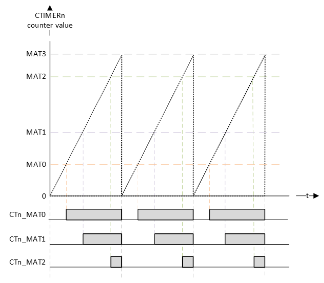
The timing diagram shows that the top value is the MAT3 register. The other MAT registers can be used for compare matches. If a match occurs, the corresponding pin will generate a rising edge. At the beginning of the PWM cycle, all channel pins will generate a falling edge (unless their match value is zero).
CTIMER configuration
The configuration of the CTIMER is done by following the initialization steps as described in the reference manual paragraph 26.1.5.
- Select a clock source for the CTIMER using MRCC_CTIMER0_CLKSEL, MRCC_CTIMER1_CLKSEL, and MRCC_CTIMER2_CLKSEL registers.
- Enable the clock to the CTIMER via the CTIMERGLOBALSTARTEN[CTIMER0_CLK_EN], CTIMERGLOBALSTARTEN[CTIMER1_CLK_EN], and CTIMERGLOBALSTARTEN[CTIMER2_CLK_EN] fields. This enables the register interface and the peripheral function clock.
- Clear the CTIMER peripheral reset using the MRCC_GLB_RST0 registers.
- Each CTIMER provides interrupts to the NVIC. See MCR and CCR registers in the CTIMER register section for match and capture events. For interrupt connections, see the attached NVIC spreadsheet.
- Select timer pins and pin modes as needed through the relevant PORT registers.
- The CTIMER DMA request lines are connected to the DMA trigger inputs via the DMAC0_ITRIG_INMUX registers (See Memory map and register definition). Note that timer DMA request outputs are connected to DMA trigger inputs.
As an example, a CTIMER1 will be used to create a PWM signal for dimming the red RGB LED to 10%. The PWM signal of will get a frequency of 1kHz. This doesn't require the use of interrupts or DMA requests, so steps 4. and 6. can be omitted. The other steps are explained in more detail in the following sections.
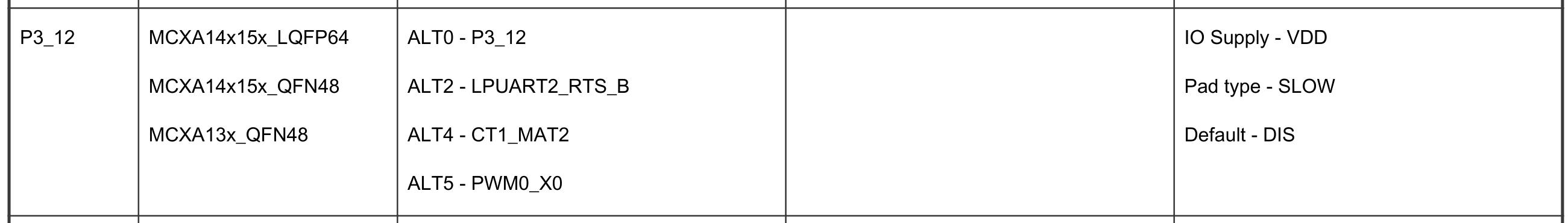
The red RGB LED is connected to P3_12. The reference manual shows that this pin is connected to CTIMER1 match register channel 2 (CT1_MAT2). This is mux alternative 4 (ALT4).
1. Select a clock source
The source clock is selected in the MRCC module. From the available options, 1MHz is selected. Furthermore, the source clock is configured to run and the divider is set to 1. This divider can be seen as an additional prescaler (available in the MRCC module).
// MUX: [101] = CLK_1M
MRCC0->MRCC_CTIMER1_CLKSEL = MRCC_MRCC_CTIMER1_CLKSEL_MUX(0b101);

// HALT: [0] = Divider clock is running
// RESET: [0] = Divider isn't reset
// DIV: [0000] = divider value = (DIV+1) = 1
MRCC0->MRCC_CTIMER1_CLKDIV = 0;
2. Enable the clock to the CTIMER
The CTIMER module interface and function clock are disabled by default. These are enabled in the SYSCON module as follows:
// CTIMER1_CLK_EN: [1] = CTIMER 1 function clock enabled
SYSCON->CTIMERGLOBALSTARTEN |= SYSCON_CTIMERGLOBALSTARTEN_CTIMER1_CLK_EN(1);
3. Clear the CTIMER peripheral reset
Similar to all other modules, the CTIMER needs to be enabled and released from reset in the MRCC module:
// Enable modules and leave others unchanged
// CTIMER1: [1] = Peripheral clock is enabled
MRCC0->MRCC_GLB_CC0_SET = MRCC_MRCC_GLB_CC0_CTIMER1(1);

// Release modules from reset and leave others unchanged
// CTIMER1: [1] = Peripheral is released from reset
MRCC0->MRCC_GLB_RST0_SET = MRCC_MRCC_GLB_RST0_CTIMER1(1);
5. Select timer pins and pin modes
By setting a prescaler of 10, the f_counter = 1 MHz / 10 = 100 kHz.
If the top (MAT3) value is set to (100-1), then f_pwm = 100 kHz / 100 = 1 kHz.
It also means that valid match register values are 0 to 100. So the precision of the PWM duty cycle is 100 steps.
Setting a duty cycle of 10% is done by writing 10 to the MAT2 register.
// Specifies the prescale value. 1 MHz / 10 = 100 kHz
CTIMER1->PR = 10-1;

// Match value: 100 kHz / 100 = 1 kHz
//
// In PWM mode, use match channel 3 to set the PWM cycle length. The other
// channels can be used for matches
CTIMER1->MR[2] = 10;
CTIMER1->MR[3] = 100-1;
Furthermore, the the three bits for each channel must be configured:
// MR2S: [0] = Does not stop Timer Counter (TC) if MR0 matches Timer Counter
//             (TC)
// MR2R: [0] = Resets Timer Counter (TC) if MR0 matches its value.
// MR2I: [0] = No interrupt when MR0 matches the value in Timer
//             Counter (TC).
// MR3S: [0] = Does not stop Timer Counter (TC) if MR3 matches Timer Counter
//             (TC)
// MR3R: [1] = Resets Timer Counter (TC) if MR3 matches its value.
// MR3I: [0] = No interrupt when MR3 matches the value in Timer
//             Counter (TC).
CTIMER1->MCR |= CTIMER_MCR_MR3R(1);
Plus the fact that PWM mode of operation is selected for channels 2 and 3:
// Configure match outputs as PWM outputs.
CTIMER1->PWMC |= CTIMER_PWMC_PWMEN3(1) | CTIMER_PWMC_PWMEN2(1);
The pin P3_12 must be configured for muxing slot alternative 4 as follows:
// Enable modules and leave others unchanged
// PORT3: [1] = Peripheral clock is enabled
MRCC0->MRCC_GLB_CC1_SET = MRCC_MRCC_GLB_CC1_PORT3(1);

// Release modules from reset and leave others unchanged
// PORT3: [1] = Peripheral is released from reset
MRCC0->MRCC_GLB_RST1_SET = MRCC_MRCC_GLB_RST1_PORT3(1);

// Configure P3_12
// LK : [1] = Locks this PCR
// INV: [0] = Does not invert
// IBE: [0] = Disables
// MUX: [0100] = Alternative 4 (CT1_MAT2)
// DSE: [0] = low drive strength is configured on the corresponding pin,
//            if the pin is configured as a digital output
// ODE: [0] = Disables
// SRE: [0] = Fast
// PE:  [0] = Disables
// PS:  [0] = n.a.
PORT3->PCR[12] = PORT_PCR_LK(1) | PORT_PCR_MUX(4);
And finally, the timer is enabled:
// CEN: [1] = Enables the counters.
CTIMER1->TCR |= CTIMER_TCR_CEN(1);
The theoretical result is depicted in the following timing diagram:
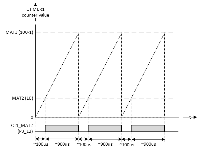
FYI: the RGB LEDs are on when the pin is logic 0.
Checking the actual generated signal with a logic analyzer:
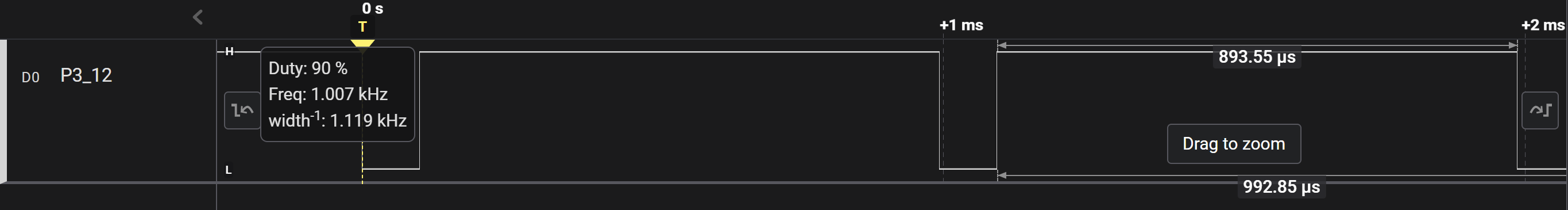
One thing to notice is that the CTIMER always generates inverted PWM signal (active low PWM)! In the example above this is not a problem, because the LEDs are on with logic 0. There is no configuration option to invert the generated PWM signal.
Assignment
Q1 In the example, the red LED was chosen and not the blue or green LED for a specific reason. Can you figure out that reason? Tip: look at the alternative functions of the pins.
Q2 What happens if you write 0 to MAT2?
Q3 What happens if you write 50 to MAT2?
Q4 What happens if you write 100 to MAT2?
Q5 What happens if you write 150 to MAT2?
Q6 What happens if the prescaler is changed from 10 to 1?
Q7 With the prescaler set to 0, what should be the value of MAT3 to maintain a 1 kHz PWM signal?
Q8 What is a benefit of a higher input frequency?
Assignment - Servo motor
Resources: ese_shieldv3_examples\servo\ctimer
Goal
To practice with the modules discussed so far.
Hardware requirements
- FRDM-MCXA153 board
- Servo motor, can conveniently be connected to the Shield V3 or by using three jumper wires.
- Type-C USB cable
Functional requirements
The application uses a servo motor connected to P3_10. A CTimer must be used to control the servo motor PWM pulse width with 1000 steps precision.
Architecture
The Shield V3 shows an example of how to connect the hardware parts.
A servo motor typically requires a PWM frequency of 50 Hz and a duty cycle between 1 and 2 ms. as depicted in the following image:
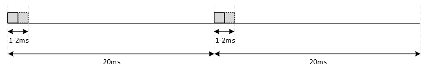
API
In order to create the functional requirements, the following API functions are prepared.
/*!
 * \brief Initializes the servo pins
 *
 * Resources:
 * - SERVO_PWM | P3_10 | CT1_MAT0
 *
 * Configures CTimer1 to generate a PWM signal on MAT0 with a 50 Hz frequency.
 */
void servo_init(void);

/*!
 * \brief Set the servo duty cycle
 *
 * Sets the PWM duty cycle as follows:
 * - 1000 =   0% = 1.0 ms pulse width = servo moves left
 * - 1500 =  50% = 1.5 ms pulse width = servo moves centre
 * - 2000 = 100% = 2.0 ms pulse width = servo moves right
 *
 * \param[in]  value Duty cycle of the PWM signal
 */
void servo_set(int32_t value);
Implementation tips
- Use the reference manual to find out what CTIMER and what match register are connected to P3_10.
- The functional requirements state that the PWM pulse must be controlled with 1000 steps precision. This means that if 1 ms must be divided in 1000 steps, 20 ms must be divided in 20000 steps. And thus, 1 second must be divided in one million steps.
- A CTimer generates an active low PWM signal, whereas the servo motor requires an active high PWM signal. There is no configuration option in the CTimer to generate an inverted PWM, so a software solution needs to be constructed. Tip: match_register = (top - value).
- Use a logic analyzer to verify the generated PWM signal.
Low-Power UART - polling
Resources: ese_driver_examples\lpuart\polling
Goal
To know how to configure the LPUART for basic serial communication and use the LPUART by polling bits in the status register.
LPUART features
The MCXA153 has three instances of the LPUART module. These are called LPUART0, LPUART1 and LPUART2. The LPUART is described in the reference manual chapter 37.
The MCU-Link on the FRDM-MCXA153 supports the VCOM serial port feature, which adds a serial COM port on the host computer and connects it to the target MCU while working as a USB-to-UART bridge.
Refer to board schematic page 6. It shows that the following pins are connected to the MCU-Link:
- P0_2 - LPUART0_RXD
- P0_3 - LPUART0_TXD
The PORT module must be used to configure the function for a pin. The reference manual paragraph 10.3 can be used to find the alternative functions that must be selected for both these pins:
- P0_2 - LPUART0_RXD - ALT2
- P0_3 - LPUART0_TXD - ALT2
LPUART configuration
There are a lot of configuration options for he LPUART, however, configuring the LPUART for straight forward 8 data bit, no parity and 1 stop bit communication, is relatively easy.
The steps to take are:
- Configure clock source in the MRCC module
- Enable modules in the MRCC module
- Configure alternate function in the PORT module
- Set baud rate (depending on clock source) in the LPUART module
- Enable receiver and/or transmitter in the LPUART module
These steps are explained in more detail in the following sections.
1. Configure clock source
// Set clock source
// MUX: [010] = FRO_HF_DIV (defaults: FRO_HF = 48 MHz; DIV = 1)
MRCC0->MRCC_LPUART0_CLKSEL = MRCC_MRCC_LPUART0_CLKSEL_MUX(0b010);

// HALT: [0] = Divider clock is running
// RESET: [0] = Divider isn't reset
// DIV: [0000] = divider value = (DIV+1) = 1
MRCC0->MRCC_LPUART0_CLKDIV = 0;
2. Enable modules
// Enable modules and leave others unchanged
// LPUART0: [1] = Peripheral clock is enabled
// PORT0: [1] = Peripheral clock is enabled
MRCC0->MRCC_GLB_CC0_SET = MRCC_MRCC_GLB_CC0_LPUART0(1);
MRCC0->MRCC_GLB_CC0_SET = MRCC_MRCC_GLB_CC0_PORT0(1);

// Release modules from reset and leave others unchanged
// LPUART0: [1] = Peripheral is released from reset
MRCC0->MRCC_GLB_RST0_SET = MRCC_MRCC_GLB_CC0_LPUART0(1);
MRCC0->MRCC_GLB_RST0_SET = MRCC_MRCC_GLB_CC0_PORT0(1);
3. Configure alternate function
// Configure P0_2
// LK : [1] = Locks this PCR
// INV: [0] = Does not invert
// IBE: [1] = Digital Input Buffer Enable, otherwise pin is used for analog
//            functions
// MUX: [0010] = Alternative 2 - LPUART0_RXD
// DSE: [0] = low drive strength is configured on the corresponding pin,
//            if the pin is configured as a digital output
// ODE: [0] = Disables
// SRE: [0] = Fast
// PE:  [0] = Disables
// PS:  [0] = n.a.
PORT0->PCR[2] = PORT_PCR_LK(1) | PORT_PCR_MUX(2) | PORT_PCR_IBE(1);

// Configure P0_3
// LK : [1] = Locks this PCR
// INV: [0] = Does not invert
// IBE: [0] = Input buffer disable
// MUX: [0010] = Alternative 2 - LPUART0_TXD
// DSE: [0] = low drive strength is configured on the corresponding pin,
//            if the pin is configured as a digital output
// ODE: [0] = Disables
// SRE: [0] = Fast
// PE:  [0] = Disables
// PS:  [0] = n.a.
PORT0->PCR[3] = PORT_PCR_LK(1) | PORT_PCR_MUX(2);
4. Set baud rate
The baud rate is set in the LPUART->BAUD register by the OSR and SBR bit fields. This register is described in the reference manual.
- OSR configures the oversampling ratio. The reset value is 0b01111, which results in an OSR of 16.
- SBR sets the modulo divide rate for the baud rate generator. The reset value is 0b0000000000100.
The reference manual description for SBR also shows the formula for calculating the baud rate:
// baud rate = baud clock / ((OSR + 1) * SBR)
//
// Rewritten: SBR = baud clock / (baud rate * (OSR+1))
In this formula, the baud clock is set in the MRCC in step 1., which in this example is set to 48 MHz.
// Configure baud rate
// OSR: [01111] = Results in an OSR of 16 (15+1)
// SBR: [.............] = baud rate = baud clock / ((OSR + 1) * SBR)
//                        => SBR = baud clock / (baud rate * (OSR+1))
LPUART0->BAUD = LPUART_BAUD_OSR(0b01111) |
    LPUART_BAUD_SBR(CLK_FRO_48MHZ / (baudrate * 16));
5. Enable receiver and/or transmitter
The receiver and transmitter are enabled in the LPUART0->CTRL register.
// TE: [1] = Transmitter Enable
// RE: [1] = Receiver Enable
LPUART0->CTRL |= LPUART_CTRL_TE(1) | LPUART_CTRL_RE(1);
Putting a character
A polling function for putting a character is implemented by checking the Transmit Data Register Empty Flag (TDRE). A while-loop waits as long as the transmit data register is empty.
void lpuart0_putchar(const int data)
{
    while((LPUART0->STAT & LPUART_STAT_TDRE_MASK) == 0)
    {}

    LPUART0->DATA = (uint8_t)data;
}
Getting a character
A polling function for getting a character is implemented by checking the Receive Data Register Full Flag (RDRF). A while-loop waits as long as the receive data register is not full.
int lpuart0_getchar(void)
{
    while((LPUART0->STAT & LPUART_STAT_RDRF_MASK) == 0)
    {}

    return (uint8_t)(LPUART0->DATA);
}
Final assignment
None.
Extra: retarget IO
The functions lpuart0_putchar() and lpuart0_getchar() can be used for sending and receiving individual characters. But what if you wanted to print a 32-bit integer in hexadecimal format? In that case, it would be very convenient to have the stdio functions for formatting input and output, such as printf(). This is possible and is called retargeting IO.
IO formatting functions, such as printf(), are part of the C standard library. These libraries can be implemented in different ways, for example by taking special considerations when dealing with the limited resources on embedded systems. When using a function from such a library, it is added to the executable by the linker.
Some examples of C standard libraries are:
- Microsoft C run-time library
- GNU C Library
- Newlib C standard library
- Newlib nano C standard library
- Redlib
Depending on the installed toolchain, one or more of these libraries might be available. Selecting a library is done in the project settings.
When using printf(), for example, on an embedded device without display, where should the printed string be displayed? The C standard libraries have an option to overwrite the built in read() and write() functions. These functions are declared so-called weak, which allows a developer to write his own functions. In these functions, IO can be retargeted to a specific interface, such as a UART, display, and/or USB. Different libraries may require different read() and write() functions.
For example:
- In Newlib these functions are:
int _write(int fd, const void *buf, size_t count);
int _read(int fd, const void *buf, size_t count);
- In Redlib these functions are:
int __sys_write(int handle, char *buffer, int size);
int __sys_readc(void);
- In MDK-ARM these functions are:
int stdout_putchar(int ch);
int stdin_getchar(void);
These functions have been implemented in the file retarget.c. Notice the use of the defines MDKARM, __NEWLIB__, and __REDLIB__, for conditional compilation for more than one C standard library.
#ifdef MDKARM

// Functions for redirecting standard output to LPUART0 for
// the ARM C libraries (used for example in MDK-ARM)

int stdout_putchar(int ch)
{
    lpuart0_putchar(ch);
    return ch;
}

int stdin_getchar(void)
{
    return lpuart0_getchar();
}

#endif

#ifdef __NEWLIB__

// Functions for redirecting standard output to LPUART0 for
// the Newlib C standard library

int _write(int fd, const void *buf, size_t count)
{
    (void)fd;

    for(size_t i=0; i<count; i++)
    {
        lpuart0_putchar(((char *)buf)[i]);
    }

    return count;
}

int _read(int fd, const void *buf, size_t count)
{
    (void)fd;

    for(size_t i=0; i<count; i++)
    {
        ((char *)buf)[i] = lpuart0_getchar();
    }

    return count;
}

#endif

#ifdef __REDLIB__

// Functions for redirecting standard output to LPUART0 for
// the Redlib C standard library

int __sys_write(int handle, char *buffer, int size)
{
    if (NULL == buffer)
    {
        // return -1 if error
        return -1;
    }

    // This function only writes to "standard out" and "standard err" for
    // all other file handles it returns failure
    if ((handle != 1) && (handle != 2))
    {
        return -1;
    }

    // Send data
    for(size_t i=0; i<size; i++)
    {
        lpuart0_putchar(((char *)buffer)[i]);
    }

    return size;
}

int __sys_readc(void)
{
    return lpuart0_getchar();
}

#endif
C standard libraries for embedded systems tend to have printing of floating point numbers disabled. The following sections describe how to do this for MCUXpresso-IDE and MCUXpresso for VSCode.
MCUXpresso-IDE
MCUXpresso-IDE projects use Redlib by default. Two defines need to be updated in the project settings as depicted below:
- Delete the define CR_INTEGER_PRINTF
- Set PRINTF_FLOAT_ENABLE=1

MCUXpresso for VSCode
MCUXpresso for VSCode projects use Newlib by default.
- Open the file armgcc\flags.cmake
- Find the following:
IF(NOT DEFINED SPECS)
    SET(SPECS "--specs=nano.specs --specs=nosys.specs")
ENDIF()
- Add the linker flags
-u _printf_floatas follows:
IF(NOT DEFINED SPECS)
    SET(SPECS "--specs=nano.specs -u _printf_float --specs=nosys.specs")
ENDIF()
Note: In general, stdio printing (such as printf()), should not be performed in an interrupt handler!
Low-Power UART - interrupt
Resources: ese_driver_examples\lpuart\interrupt
Goal
To understand what it takes to use the LPUART with interrupts when compared to polling.
Interrupts instead of polling
Using LPUART transmitter and receiver interrupts is actually pretty straight forward, as soon as polling has been implemented:
- Enable the interrupts in the LPUART0->CTRL register.
- Enable LPUART0 interrupts in the NVIC and set priority.
- Implement an interrupt handler called LPUART0_IRQHandler().
The hard part is to implement a data structure to:
- Temporary store incoming data
- Temporary store outgoing data
Circular buffer
One way to implement a data structure for storing data is a circular buffer. One advantage is that it uses static memory, of which the size is set at compile time. This makes it a fast implementation, when, for example, compared to a dynamically allocated singly linked list.
The circular buffer is implemented in the files fifo.c and fifo.h.
Putting a character
Transmitter interrupts are disabled by default. Putting a character takes the following steps:
- Append the character to the transmit fifo.
- Enable transmit interrupts.
- Wait for the interrupt to occur. In the interrupt handler, read data from the transmit fifo and transmit this data via the LPUART0->DATA register.
- If there is no more data, disable transmit interrupts.
Q1 Examine the file lpuart0_interrupt.c. Relate all of these steps to the respective line(s) of code.
Q2 What will happen if the transmit fifo is full?
Getting a character
Receive interrupts are enabled by default. Getting a character takes the following steps:
- Wait for an interrupt to occur. In the interrupt handler, read data from the LPUART0->DATA register and put it in the receive fifo.
- Provide a function to check if data is available in the receive fifo.
- If data is read, return the first item from the fifo.
Q3 Examine the file lpuart0_interrupt.c. Relate all of these steps to the respective line(s) of code.
Q4 Examine the file lpuart0_interrupt.c. What will happen if the receive fifo is full?
Assignment
Q5 At 115200-8n1, how long does it take to transmit 1024 bytes?
Implement a driver to support LPUART2. Proceed as follows:
- Copy the file lpuart0_interrupt.h and rename it to lpuart2_interrupt.h.
- Copy the file lpuart0_interrupt.c and rename it to lpuart2_interrupt.c.
- Add both files to the project (as applicable for the IDE).
- Rewrite all functions and function prototypes to support LPUART2. Configure the pins as follows and make sure the correct alternative function is selected:
- LPUART2_RXD - P1_4
- LPUART2_TXD - P1_5
Test the implementation as follows:
- Connect a jumper wire from P1_4 to P1_5. All data transmitted by UART2 will thus be received by UART2.
- Replace the main() function in main.c with the following:
int main(void)
{
    gpio_output_init();
    lpuart0_init(115200);
    lpuart2_init(115200);

    printf("LPUART0 and LPUART2 Interrupt");
    printf(" - %s\r\n", TARGETSTR);
    printf("Build %s %s\r\n", __DATE__, __TIME__);

    while(1)
    {
        if(lpuart0_rxcnt() > 0)
        {
            int data = lpuart0_getchar();
            lpuart2_putchar(data);
        }

        if(lpuart2_rxcnt() > 0)
        {
            int data = lpuart2_getchar();
            lpuart0_putchar(data);
        }
    }
}
- Build and run the application.
- Open the VCOM (115200-8n1) in a terminal application of your choice. Transmit several characters. All characters that are transmitted will also be received in the terminal application.
- Disconnect the jumper wire from P1_4 to P1_5.
- In the same terminal application, transmit several characters. All characters that are transmitted will not be received in the terminal application anymore.
- Connect the jumper wire from P1_4 to P1_5.
- Connect a logic analyzer to the jumper wire.
- Transmit several characters.
- Visualize these characters by using an analyzer that decodes the signal to an ASCII representation.
Low-Power UART - DMA
Resources: ese_driver_examples\lpuart\dma
Goal
To understand what DMA is.
To understand what it takes to use the LPUART with DMA.
Direct Memory Access
A Direct Memory Access (DMA) controller is capable of performing data transfers with minimal intervention of the host processor. This is depicted in the following simplified bus matrix diagram.
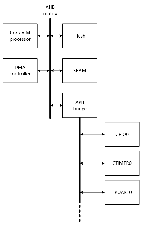
The Cortex-M processor is a master on the Advanced High-performance Bus (AHB). It initiates transfers from one location to the other. For example, when reading data from a UART register through the Advanced Peripheral Bus (APB), into a memory location in SRAM. This means that for simple tasks, such as moving data, the processor is busy.
Instead of letting the processor move data, the DMA controller can take care of that. This offloads the processor, so the processor can execute other instructions at the same time.
The reference manual paragraph 4.1 shows the more detailed bus matrix block diagram of the MCXA153 microcontroller:
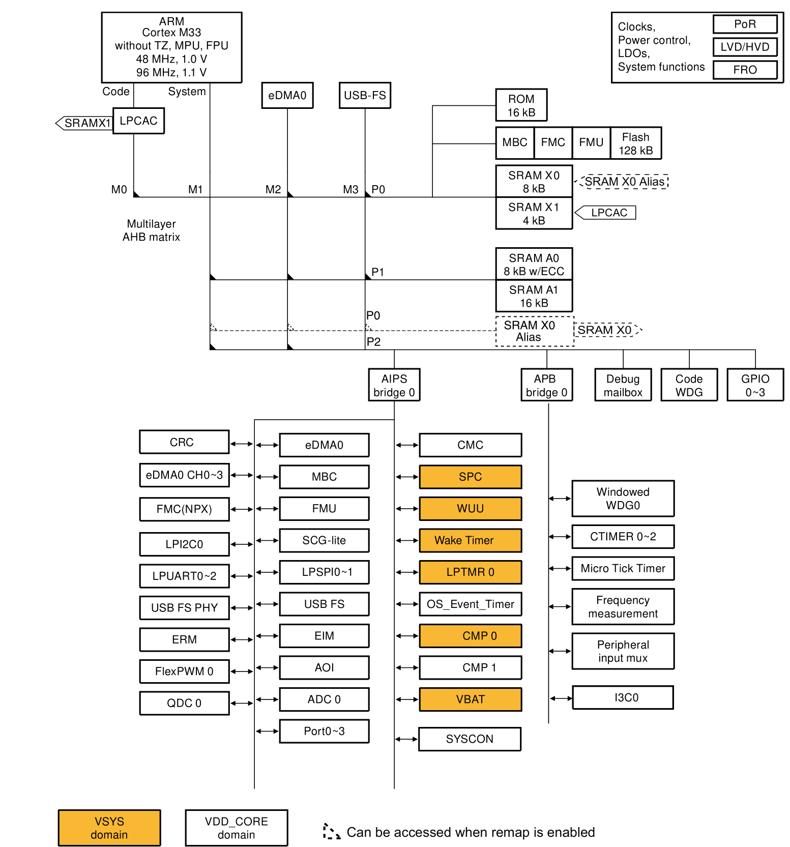
The figure shows a multilayer interconnection scheme that allows for parallel communication between multiple masters and slaves. Each master has its dedicated AHB layer that connects to all the slave devices. For a firmware developer this is transparent. In other words, the firmware developer can address a peripheral or a memory location by reading/writing a memory location.
Enhanced DMA Controller
The MCXA153 microcontroller has one so-called Enhanced DMA Controller (eDMA). It is described in chapter 15 of the reference manual.
The DMA controller is called eDMA0 and features four channels. This means it can be configured to move data from/to four source/destination pairs.
The eDMA module consists of two major subsystems:
- The eDMA engine
- The eDMA local memory that describes the transfer control for each channel. This is a.k.a. the Transfer Control Descriptors (TCD).
Features of the eDMA module are:
- Programmable source and destination addresses and transfer size
- Support for complex address calculations
- Internal data buffer, used as temporary storage for all transfers
- Channel activation via one of three methods:
- Explicit software initiation
- Initiation via a channel-to-channel linking mechanism for continuous transfers
- Peripheral-paced hardware requests, one per channel
- Channel completion reported via programmable interrupt requests
A simplified block diagram of the eDMA module is depicted below:
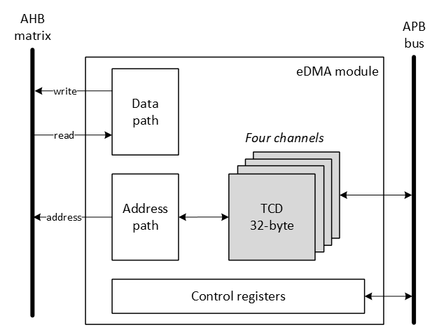
The eDMA module is configured through its Control registers and the four TCDs. Once configured, for each transfer it will:
- control the source and destination addresses
- read data from the source
- internally buffer the data if required
- write the data to the destination
- calculate the new source and destination addresses or optionally generates an interrupt when the transfer is finished
eDMA example: LPUART data transmission
This example demonstrates how to send a string of characters with the UART by using the DMA controller. Pins P0_2 (LPUART0_RXD) and P0_3 (LPUART0_TXD) will be used for UART signals. The DMA controller should generate an interrupt as soon as the transfer is finished.
The following needs to be configured initially:
- Enable modules
- LPUART0
- PORT0
- eDMA0
- Configure P0_2 and P0_3 pin functions
- Configure UART0
-
Associate the DMA channel with the UART0 peripheral. For this purpose, an Excel sheet is attached to the reference manual. It is called 'DMA_Configuration.xlsx'. Part of this table is depicted below:
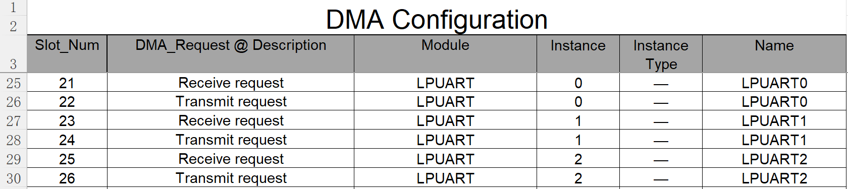
It shows, for example, that slot number 22 is the LPUART0 transmit request.
-
Enable channel interrupts
The following example shows the implementation for these steps for UART transmission with DMA channel 0.
void lpuart0_dma_init(const uint32_t baudrate)
{
    // Set clock source
    // MUX: [010] = FRO_HF_DIV (defaults: FRO_HF = 48 MHz; DIV = 1)
    MRCC0->MRCC_LPUART0_CLKSEL = MRCC_MRCC_LPUART0_CLKSEL_MUX(0b010);

    // HALT: [0] = Divider clock is running
    // RESET: [0] = Divider isn't reset
    // DIV: [0000] = divider value = (DIV+1) = 1
    MRCC0->MRCC_LPUART0_CLKDIV = 0;

    // Enable modules and leave others unchanged
    // LPUART0: [1] = Peripheral clock is enabled
    // PORT0: [1] = Peripheral clock is enabled
    // DMA: [1] = Peripheral clock is enabled
    MRCC0->MRCC_GLB_CC0_SET = MRCC_MRCC_GLB_CC0_LPUART0(1);
    MRCC0->MRCC_GLB_CC0_SET = MRCC_MRCC_GLB_CC0_PORT0(1);
    MRCC0->MRCC_GLB_CC0_SET = MRCC_MRCC_GLB_CC0_DMA(1);

    // Release modules from reset and leave others unchanged
    // LPUART0: [1] = Peripheral is released from reset
    // PORT0: [1] = Peripheral is released from reset
    // DMA: [1] = Peripheral is released from reset
    MRCC0->MRCC_GLB_RST0_SET = MRCC_MRCC_GLB_RST0_LPUART0(1);
    MRCC0->MRCC_GLB_RST0_SET = MRCC_MRCC_GLB_RST0_PORT0(1);
    MRCC0->MRCC_GLB_RST0_SET = MRCC_MRCC_GLB_RST0_DMA(1);

    // Configure P0_2
    // LK : [1] = Locks this PCR
    // INV: [0] = Does not invert
    // IBE: [1] = Digital Input Buffer Enable, otherwise pin is used for analog
    //            functions
    // MUX: [0010] = Alternative 2 - LPUART0_RXD
    // DSE: [0] = low drive strength is configured on the corresponding pin,
    //            if the pin is configured as a digital output
    // ODE: [0] = Disables
    // SRE: [0] = Fast
    // PE:  [0] = Disables
    // PS:  [0] = n.a.
    PORT0->PCR[2] = PORT_PCR_LK(1) | PORT_PCR_MUX(2) | PORT_PCR_IBE(1);

    // Configure P0_3
    // LK : [1] = Locks this PCR
    // INV: [0] = Does not invert
    // IBE: [0] = Input buffer disable
    // MUX: [0010] = Alternative 2 - LPUART0_TXD
    // DSE: [0] = low drive strength is configured on the corresponding pin,
    //            if the pin is configured as a digital output
    // ODE: [0] = Disables
    // SRE: [0] = Fast
    // PE:  [0] = Disables
    // PS:  [0] = n.a.
    PORT0->PCR[3] = PORT_PCR_LK(1) | PORT_PCR_MUX(2);

    // Configure LPUART0. Although there are a lot of configuration options, the
    // default configuration takes the following steps:
    // 1. Configure baud rate
    // 2. Enable receiver and/or transmitter

    // 1.
    //
    // Configure baud rate
    // OSR: [01111] = Results in an OSR of 16 (15+1)
    // SBR: [.............] = baud rate = baud clock / ((OSR + 1) * SBR)
    //                        => SBR = baud clock / (baud rate * (OSR+1))
    LPUART0->BAUD = LPUART_BAUD_OSR(0b01111) |
       LPUART_BAUD_SBR(CLK_FRO_48MHZ / (baudrate * 16));

    // 2.
    //
    // TE: [1] = Transmitter Enable
    LPUART0->CTRL |= LPUART_CTRL_TE(1);

    // Write a single time to this register, or it will be reset!!
    // In other words, do not update it in the function lpuart0_dma_write().
    // See 15.6.2.7:
    //     "If there is an attempt to write a mux configuration value that is
    //      already consumed by any channel, a mux configuration of 0 (SRC = 0)
    //      will be written"
    DMA0->CH[0].CH_MUX = DMA_CH_MUX_SRC(22);

    // Enable DMA channel 0 interrupts
    NVIC_SetPriority(DMA_CH0_IRQn, 3);
    NVIC_ClearPendingIRQ(DMA_CH0_IRQn);
    NVIC_EnableIRQ(DMA_CH0_IRQn);
}
For every transfer, paragraph 15.5.1 in the reference manual describes what should be done:
- Write to the MP_CSR if a configuration other than the default is wanted.
- Write the channel priority levels to the CHn_PRI registers and group priority levels to the CHn_GRPRI registers if a configuration other than the default is wanted.
- Enable error interrupts in the CHn_CSR[EEI] registers if they are wanted.
- Write the 32-byte TCD for each channel that may request service.
- Enable any hardware service requests via the CHn_CSR[ERQ] registers.
- Request channel service via either:
- Software: setting TCDn_CSR[START]
- Hardware: slave device asserting its eDMA peripheral request signal
Steps 1. to 3. are not required in a 'simple' UART requested DMA transfer. The other steps are explained in more detail in the following sections. An overview of what needs to be eabled is provided in the following image:
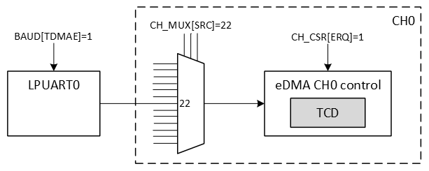
For a detailed description of a single request transfer, also see paragraph 15.5.5.1 of the reference manual.
4. Write the 32-byte TCD
The fields of the TCD are depicted in the following image (taken from the reference manual):
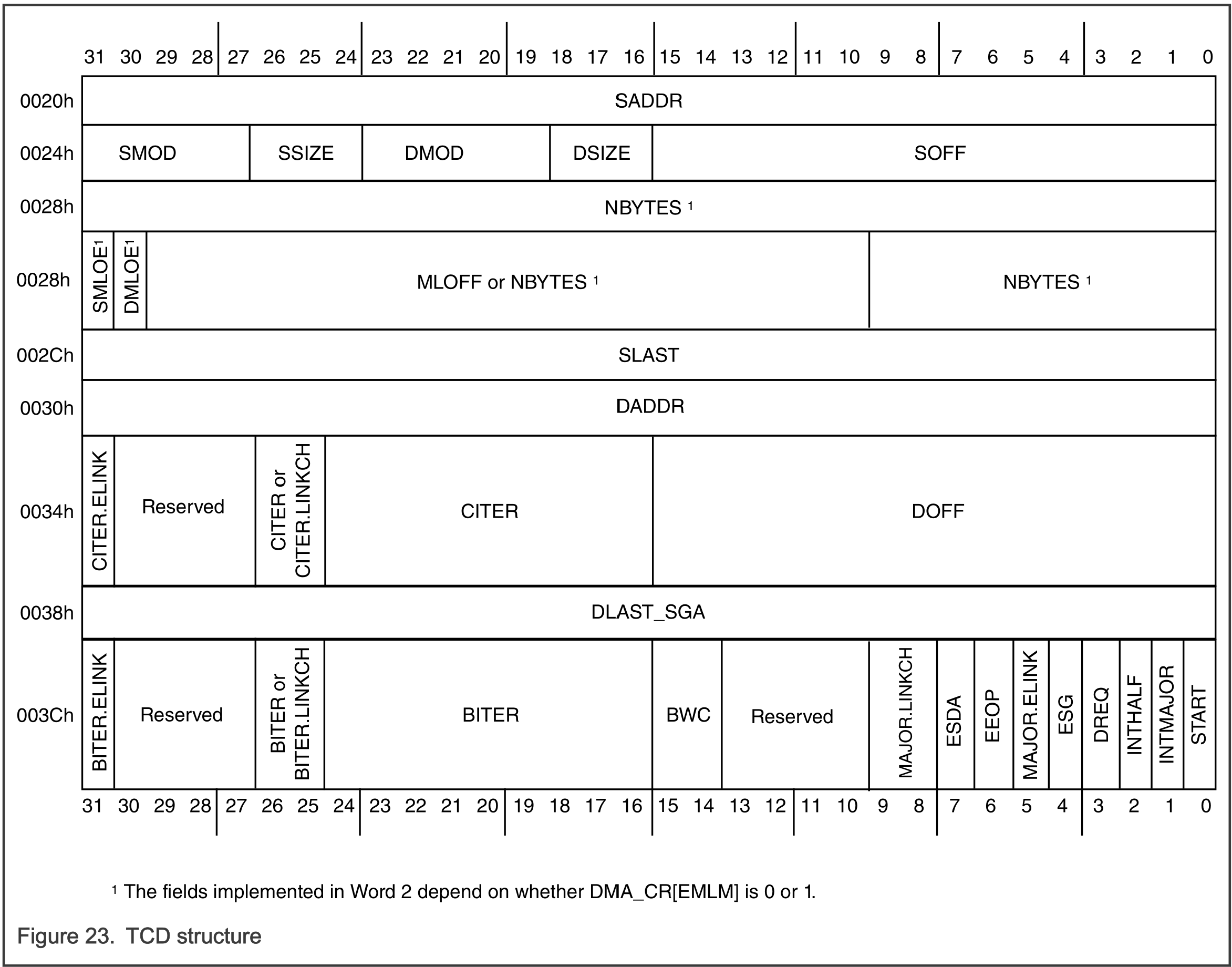
The following code snippet shows how to configure a transfer of n-bytes from a buffer in RAM to the UART data register:
// Source and destination address
DMA0->CH[0].TCD_SADDR = (uint32_t)buffer;
DMA0->CH[0].TCD_DADDR = (uint32_t)(&(LPUART0->DATA));

// Source address: +1
// Destination address: +0
DMA0->CH[0].TCD_SOFF = DMA_TCD_SOFF_SOFF(1);
DMA0->CH[0].TCD_DOFF = DMA_TCD_DOFF_DOFF(0);

// For both source and destination: modulo feature disabled and
// 8-bit transfers
DMA0->CH[0].TCD_ATTR = DMA_TCD_ATTR_SMOD(0) | DMA_TCD_ATTR_SSIZE(0) |
                       DMA_TCD_ATTR_DMOD(0) | DMA_TCD_ATTR_DSIZE(0);

// Transfer one byte per service request
DMA0->CH[0].TCD_NBYTES_MLOFFNO = 1;

// No address adjustments at the end of the major loop
DMA0->CH[0].TCD_SLAST_SDA = DMA_TCD_SLAST_SDA_SLAST_SDA(0);
DMA0->CH[0].TCD_DLAST_SGA = DMA_TCD_DLAST_SGA_DLAST_SGA(0);

// Major loop count (beginning and current): number of bytes
DMA0->CH[0].TCD_BITER_ELINKNO = n;
DMA0->CH[0].TCD_CITER_ELINKNO = n;

// Enable Interrupt if major loop count complete
DMA0->CH[0].TCD_CSR = DMA_TCD_CSR_INTMAJOR(1);
5. Enable any hardware service requests
The hardware service requests need to be enabled in the control registers of the eDMA (not the TCD).
DMA0->CH[0].CH_CSR |= DMA_CH_CSR_ERQ(1);
6. Request channel service
Channel service needs to be requested by the LPUART0, as soon as the transmit data register is empty. This is enable as follows:
// TDMAE : [1] = Enables STAT[TDRE] to generate a DMA request
LPUART0->BAUD |= LPUART_BAUD_TDMAE_MASK;
Interrupt handling
An interrupt handler is available for each channel. The following interrupt handler shows how to clear the interrupt flag, disable the UART transmit DMA request and set the global variable dma_write_done to indicate to the main application that the transfer is finished.
void DMA_CH0_IRQHandler(void)
{
    NVIC_ClearPendingIRQ(DMA_CH0_IRQn);

    DMA0->CH[0].CH_INT = DMA_CH_INT_INT_MASK;

    LPUART0->BAUD &= ~LPUART_BAUD_TDMAE_MASK;

    dma_write_done = true;
}
Assignment
None.
I2C Introduction
Resources: none
Goal
To understand the I2C communication protocol.
Communication protocol
The I2C interface is invented by Philips in the 80’s. It is used to connect several low speed peripheral devices to a microcontroller/computer with a two wire interface. With the I2C interface each device can be master and/or slave because both lines are bidirectional. Since I2C specification revision 7.0 this terminology was updated to controller and target.
The interface consists of two physical connections called Serial Data (SDA) and Serial Clock (SCL). The signals use open-drain I/O's, so external pullup resistors must be added to make sure that a logic 1 equals Vdd.
I2C is a multi-controller and multi-target interface. This implies that there must be an addressing mechanism. The following figure shows the interconnections to an I2C bus.
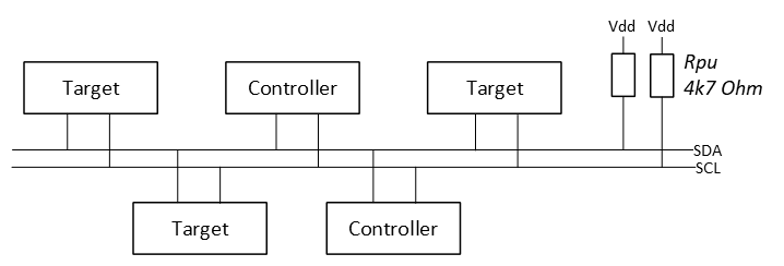
The I2C protocol states that a controller initiates a data transfer with a so-called ‘START condition’ and then immediately transmits the target address. If there are multiple I2C targets present on the same bus, only the addressed target will respond.
The address is coded in 7-bits (or 10-bits) and an additional bit (LSB) is added to let the target know what the controller wants:
- LSB = logic 0: the controller wants to write data to the target
- LSB = logic 1: the controller wants to read data from the target
In rest, both SDA and SCL are high (Vdd). The following will happen when a controller initiates an I2C transfer:
- A START condition is generated by the controller, meaning the SDA line will be pulled low while the SCL is still high (see most left green dot in the figure below).
- Then, with the frequency of SCL, 8-bit data will be transferred to all targets, but only the target with the matching hardware address will respond, accordingly the LSB (read or write). In the example below, a write transfer is initiated to a target with address 0x48.
- This transfer is acknowledged by the target device. During the ninth clock pulse it will pull down the SDA line. This is also known as the ACK bit. Then a new transfer can be initiated by the controller, in the example below 0x01 is transmitted to the target. This transfer is also acknowledged by the target.
- More data can be transferred and each transfer will be acknowledged by the target. In this example 0x28.
- After the last transfer the controller will generate a STOP condition, meaning the SDA line is released (rising edge) by the controller while leaving the SCL high (see the red square in the figure below).
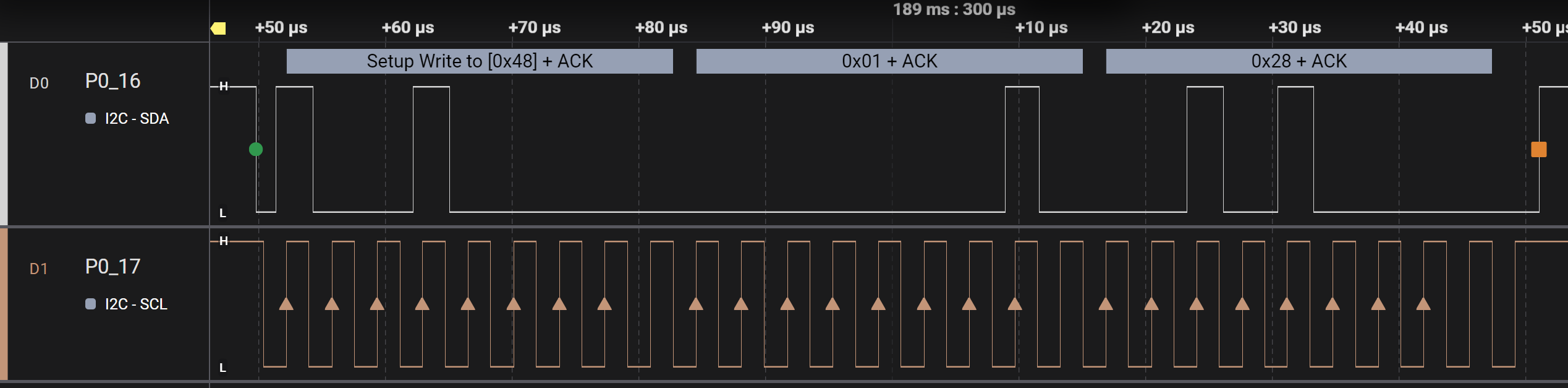
Reading from an I2C target is a little different. Before reading, the controller needs to tell the target what it wants to read. This means an initial write operation, followed immediately by a read operation.
So the following will happen when a controller initiates an I2C transfer for reading data:
- The first three steps are the same as above:
- START condition
- transmit address + write (LSB=0)
- ACK by target
- Instead of a new transfer, a so-called REPEATED START condition is generated (the second green dot in the figure below).
- The same target address is transmitted, however, now with the LSB set (LSB=1), indicating that the controller wants to read data from the target.
- This is ACKnowledged by the target.
- Next, the controller generates 8 clock pulses and the target will write data on the SDA line. This is 0x28 in the figure below.
- The data is not acknowledge, because it is transmitted by the target.
- After the last transfer the controller will generate a STOP condition (the red square in the figure below).
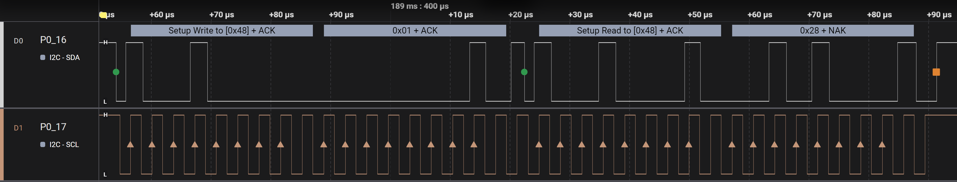
What happens if there is no device with the transmitted address on the I2C bus? The controller sends the address + R/W, but there will be no ACK as depicted in the following image:
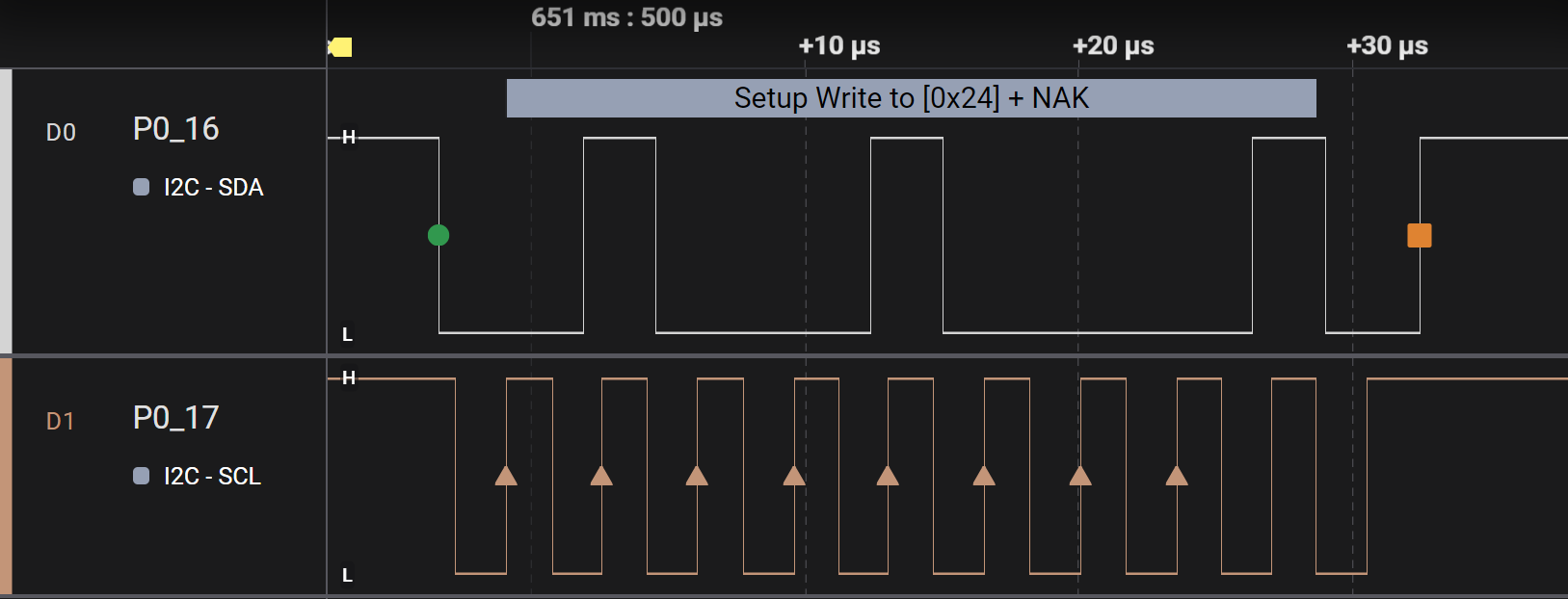
LPI2C Controller example - polling
Resources: ese_driver_examples\lpi2c\controller_polling_p3t1755
Goal
To know how to configure the Low-Power I2C module for basic serial communication and use the LPI2C by polling bits in the status register.
Pin initialization
The FRDM-MCXA153 board contains the P3T1755 digital temperature sensor. The board schematic page 7 shows the following pin connections:
- P0_16: LPI2C0_SDA
- P0_17: LPI2C0_SCL
The initialization of these required modules is as follows:
// Set clock source
// MUX: [010] = FRO_HF_DIV
MRCC0->MRCC_LPI2C0_CLKSEL = MRCC_MRCC_LPI2C0_CLKSEL_MUX(2);

// HALT: [0] = Divider clock is running
// RESET: [0] = Divider isn't reset
// DIV: [0000] = divider value = (DIV+1) = 1
MRCC0->MRCC_LPI2C0_CLKDIV = 0;

// Enable modules and leave others unchanged
// LPI2C0: [1] = Peripheral clock is enabled
// PORT0: [1] = Peripheral clock is enabled
MRCC0->MRCC_GLB_CC0_SET = MRCC_MRCC_GLB_CC0_LPI2C0(1);
MRCC0->MRCC_GLB_CC0_SET = MRCC_MRCC_GLB_CC0_PORT0(1);

// Release modules from reset and leave others unchanged
// LPI2C0: [1] = Peripheral is released from reset
// PORT0: [1] = Peripheral is released from reset
MRCC0->MRCC_GLB_RST0_SET = MRCC_MRCC_GLB_RST0_LPI2C0(1);
MRCC0->MRCC_GLB_RST0_SET = MRCC_MRCC_GLB_RST0_PORT0(1);

// Configure P0_16 and P0_17
// LK : [1] = Locks this PCR
// INV: [0] = Does not invert
// IBE: [1] = Digital Input Buffer Enable, otherwise pin is used for analog
//            functions
// MUX: [0010] = Alternative 2
// DSE: [0] = low drive strength is configured on the corresponding pin,
//            if the pin is configured as a digital output
// ODE: [0] = Disables
// SRE: [0] = Fast
// PE:  [1] = Enables
// PS:  [1] = Enables internal pullup resistor
PORT0->PCR[16] = PORT_PCR_LK(1) | PORT_PCR_MUX(2) | PORT_PCR_PE(1) |
    PORT_PCR_PS(1) | PORT_PCR_ODE(1) | PORT_PCR_IBE(1); // LPI2C0_SDA
PORT0->PCR[17] = PORT_PCR_LK(1) | PORT_PCR_MUX(2) | PORT_PCR_PE(1) |
    PORT_PCR_PS(1) | PORT_PCR_ODE(1) | PORT_PCR_IBE(1); // LPI2C0_SCL
I2C controller initialization
It takes the following steps to configure the I2C module as a controller, as described in the reference manual paragraph 36.5:
- Configure Controller Configuration 0 (MCFGR0) Controller Configuration 3 (MCFGR3) as required by the application.
- Configure Controller Clock Configuration 0 (MCCR0) and Controller Clock Configuration 1 (MCCR1) to satisfy the timing requirements of the I2C mode supported by the application.
- Enable controller interrupts and DMA requests as required by the application.
- Enable the LPI2C controller by writing 1 to MCR[MEN].
Step 3. is not needed, because this is a polling example. The other steps are explained in more detail in the following sections.
1. & 2. Configure Controller and clock Configuration
The I2C specification describes several modes of operation, such as Standard, Fast, Fast+, and HS. The P3T1755 supports Fast mode (see section 12 Dynamic characteristics).
Configuring a controller in a specific mode requires the configuration of several configuration registers called MCFGRn and MCCRn. The reference manual paragraph 36.6 shows a convenient table with example timing configurations for several modes. The following settings apply for Fast mode with a 48 MHz clock frequency (which was selected in the previous step with FRO_HF_DIV as the clock source).
// I2C timing parameters to setup the following specifications (see
// paragraph 36.6 (NXP, 2024)):
// I2C mode: FAST
// Clock frequency: 48 MHz
// I2C baud rate: 400 kbits/s
LPI2C0->MCFGR1 = LPI2C_MCFGR1_PRESCALE(0);
LPI2C0->MCFGR2 = LPI2C_MCFGR2_FILTSDA(1) | LPI2C_MCFGR2_FILTSCL(1);

LPI2C0->MCCR0 = LPI2C_MCCR0_DATAVD(0x0F) | LPI2C_MCCR0_SETHOLD(0x1D) |
    LPI2C_MCCR0_CLKHI(0x35) | LPI2C_MCCR0_CLKLO(0x3E);
4. Enable the LPI2C controller by writing 1 to MCR[MEN]
// MEN: [1] = Controller Enable
// Rest unchanged
LPI2C0->MCR |= LPI2C_MCR_MEN(1);
Writing data
The transmission of I2C data is not as 'simple' when compared to a UART. Where a UART module automatically adds a start-bit, stop-bit(s), etc. for each transmitted data item, this is not possible for I2C data because of the afore mentioned protocol. The embedded programmer must explicitly state what part of the protocol must be initiated by the hardware.
Generally speaking, writing a single byte to a single register in a target device in a polling implementation takes the following protocol steps:
- Wait while the I2C bus is busy.
- Clear all LPI2C status flags.
- Generate a START condition and transmit target address + w.
- Wait for it to complete.
- Transmit the register address to write to.
- Wait for it to complete.
- Transmit the data.
- Wait for it to complete.
- Generate a STOP condition.
In order to do this in the MCXA153 microcontroller, the LPI2C module has a register that is used for both I2C commands and, if applicable, the associated data. The command (CMD) consists of three bits and the DATA of eight bits:

These 11 bits share a single register called MTDR. The reference manual paragraph 36.7 describes this register in detail:
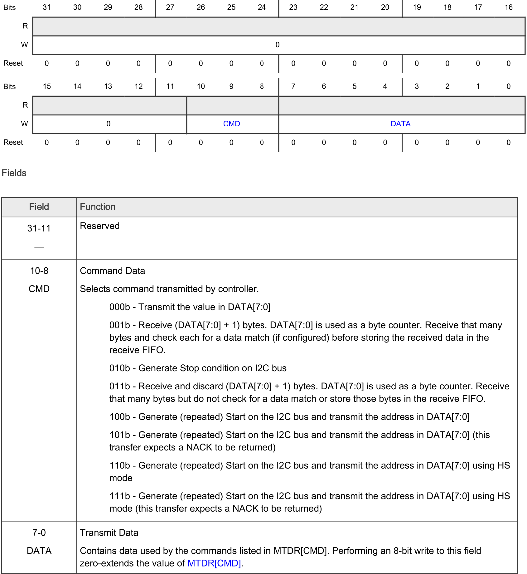
The steps 3, 5 7 and 9 are all writes to the MTDR register. In a polling implementation, the firmware must wait for the operation to complete after each write. However, the MCXA153 provides a 4 word hardware FIFO. This means the firmware can write four times to the MTDR register without having to wait for the operation to complete. This FIFO mechanism is depicted as follows:
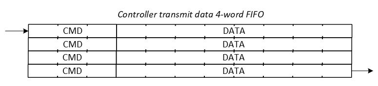
The following function is a generic function for writing data, that takes advantage of the FIFO mechanism:
void lpi2c0_write(const uint8_t dev_address, const uint8_t reg, uint8_t *p,
    const uint8_t len)
{
    // Wait as long as bus or controller is busy
    lpi2c0_wait_busy();

    // Clear all status flags
    LPI2C0->MSR = LPI2C_MSR_STF_MASK | LPI2C_MSR_DMF_MASK |
        LPI2C_MSR_PLTF_MASK | LPI2C_MSR_FEF_MASK | LPI2C_MSR_ALF_MASK |
        LPI2C_MSR_NDF_MASK | LPI2C_MSR_SDF_MASK | LPI2C_MSR_EPF_MASK;

    // Note. Four words can be written to the MTDR register, because of the
    //       four word transmit FIFO (8-bit transmit data + 3-bit command).
    //       If more must be written, use the function lpi2c0_txfifo_full()
    //       after four words to wait until the FIFO is not full anymore.

    // Command: 100b - Generate (repeated) Start on the I2C bus and transmit
    //          the address in DATA[7:0]
    // Data   : Slave address + w
    LPI2C0->MTDR = LPI2C_MTDR_CMD(0b100) | LPI2C_MTDR_DATA(dev_address);

    // Command: 000b - Transmit the value in DATA[7:0]
    // Data   : index low byte
    LPI2C0->MTDR = LPI2C_MTDR_CMD(0b000) | LPI2C_MTDR_DATA(reg);

    for(uint32_t i=0; i<len; ++i)
    {
        // Wait while transmit fifo full
        while(lpi2c0_txfifo_full())
        {}

        // Command: 000b - Transmit the value in DATA[7:0]
        // Data   : data
        LPI2C0->MTDR = LPI2C_MTDR_CMD(0b000) | LPI2C_MTDR_DATA(p[i]);
    }

    // Wait while transmit fifo full
    while(lpi2c0_txfifo_full())
    {}

    // Command: 010b - Generate Stop condition on I2C bus
    // Data   : n.a.
    LPI2C0->MTDR = LPI2C_MTDR_CMD(0b010);
}
And a PT3T1755 specific function to set the configuration register is as follows:
void p3t1755_set_configuration_reg(uint8_t val)
{
    // Device address: 0b1001000 (P3T1755)
    // Pointer byte: 0b00000001 (Configuration register)
    // Send one byte: val
    lpi2c0_write(0b1001000, 0b00000001, &val, 1);
}
Reading data
Generally speaking, reading a single byte from a single register in a target device in a polling implementation takes the following protocol steps:
- Wait while the I2C bus is busy.
- Clear all LPI2C status flags.
- Generate a START condition and transmit target address + w.
- Wait for it to complete.
- Transmit the register address to read from.
- Wait for it to complete.
- Generate a repeated START condition and transmit target address + r.
- Wait for it to complete.
- Set the number of bytes to receive to 1.
- Wait for incoming data.
- Read the incoming data.
- Generate a STOP condition.
The controller also implements a four word FIFO for the reception of data:
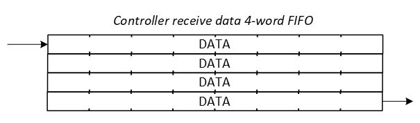
The following function is a generic function for reading data, that takes advantage of the FIFO mechanism:
void lpi2c0_read(const uint8_t dev_address, const uint8_t reg, uint8_t *p,
    const uint8_t len)
{
    // Wait as long as bus or controller is busy
    lpi2c0_wait_busy();

    // Clear all status flags
    LPI2C0->MSR = LPI2C_MSR_STF_MASK | LPI2C_MSR_DMF_MASK |
        LPI2C_MSR_PLTF_MASK | LPI2C_MSR_FEF_MASK | LPI2C_MSR_ALF_MASK |
        LPI2C_MSR_NDF_MASK | LPI2C_MSR_SDF_MASK | LPI2C_MSR_EPF_MASK;

    // Note. Four words can be written to the MTDR register, because of the
    //       four word transmit FIFO (8-bit transmit data + 3-bit command).
    //       If more must be written, use the function lpi2c0_txfifo_full()
    //       after four words to wait until the FIFO is not full anymore.

    // Command: 100b - Generate (repeated) Start on the I2C bus and transmit
    //          the address in DATA[7:0]
    // Data   : Slave address + w
    LPI2C0->MTDR = LPI2C_MTDR_CMD(0b100) | LPI2C_MTDR_DATA(dev_address << 1);

    // Command: 000b - Transmit the value in DATA[7:0]
    // Data   : index low byte
    LPI2C0->MTDR = LPI2C_MTDR_CMD(0b000) | LPI2C_MTDR_DATA(reg);

    // Command: 100b - Generate (repeated) Start on the I2C bus and transmit
    //          the address in DATA[7:0]
    // Data   : Slave address + r
    LPI2C0->MTDR = LPI2C_MTDR_CMD(0b100) | LPI2C_MTDR_DATA((dev_address << 1) | 1);

    // Command: 001b - Receive (DATA[7:0] + 1) bytes. DATA[7:0] is used as a
    //          byte counter.
    // Data   : count
    LPI2C0->MTDR = LPI2C_MTDR_CMD(0b001) | LPI2C_MTDR_DATA(len - 1);

    // Receive the data
    for(uint32_t i=0; i<len; ++i)
    {
        // Wait while the RXFIFO is empty
        while(lpi2c0_rxfifo_empty())
        {}

        // Read the data
        p[i] = (uint8_t)LPI2C0->MRDR;
    }

    // Wait while transmit fifo full
    while(lpi2c0_txfifo_full())
    {}

    // Command: 010b - Generate Stop condition on I2C bus
    // Data   : n.a.
    LPI2C0->MTDR = LPI2C_MTDR_CMD(0b010);
}
Reading the P3T1755 configuration register is thus done as follows:
uint8_t p3t1755_get_configuration_reg(void)
{
    uint8_t data = 0;

    // Device address: 0b1001000 (P3T1755)
    // Pointer byte: 0b00000001 (Configuration register)
    lpi2c0_read(0b1001000, 0b00000001, &data, 1);

    return data;
}
Notes
If polling is used, be careful that the FIFOs are 4 words. It is not possible to write more without data corruption. If more than four words need to be written to the FIFO, the firmware must wait until the FIFO is not full any more. The function lpi2c0_txfifo_full() can be used for this purpose, which checks the number of items in the MTDR FIFO by reading the MFSR register.
Another option would be to store all CMD+DATA in an array and use interrupts for the transmission. This is discussed in the next topic.
Assignment
None.
LPI2C Controller example - interrupt
Resources: ese_driver_examples\lpi2c\controller_interrupt_p3t1755
Goal
To know how to configure the Low-Power I2C module for basic serial communication and use the LPI2C with interrupts.
API
An interrutp driven API provides the advantage of not blocking the main application while waiting for a transfer to complete. The API is based on the LPI2C - polling example, but uses interrupts to handle the transmission and reception of data.
The API consists of the same functions as the LPI2C - polling example, but with the addition of the following two functions. These functions can be used to check if the transmissin has been completed or not.
void lpi2c0_write(const uint8_t dev_address, const uint8_t reg, uint8_t *p,
    const uint8_t len);
void lpi2c0_read(const uint8_t dev_address, const uint8_t reg, uint8_t *p,
    const uint8_t len);

bool lpi2c0_write_done(void);
bool lpi2c0_read_done(void);
Data validity
Similar to using an interrupt driven UART, transmitted and received data needs to be stored temporarily. Fortunately, the MCXA153A microcontroller features a LPI2C module with a four word hardware FIFO (see LPI2C - polling for more info). However, if more than four words need to be temporary stored, a software solution is required. For that purpose the interrupt driven API uses the following local variables:
static volatile uint8_t *tx_buffer; // Pointer to the buffer for transmit data
static volatile uint8_t *rx_buffer; // Pointer to the buffer for receive data
static volatile uint32_t tx_count = 0; // Number of bytes transmitted
static volatile uint32_t tx_total = 0; // Total number of bytes to transmit
static volatile uint32_t rx_count = 0; // Number of bytes received
static volatile uint32_t rx_total = 0; // Total number of bytes to receive
Notice that it uses pointers to buffers. It is the responsibility of the calling application that the data remains valid until the transmission is completed. The API does not copy the data to a local buffer.
Initialization
When compared to the LPI2C - polling example, the following additional steps are required:
- Stop condition automatically generated. The STOP condition is the last command that must be transmitted, but it cannot be appended to the user provided data buffer. However, the LPI2C module can automatically generate a stop condition when the transmit FIFO is empty and the controller is busy. This is done by setting the
STOPbit in theMCRregister. - Interrupts are enabled, in the LPI2C0 module and the NVIC.
- An interrupt handler is implemented, taking care of the transmission and reception of data.
Writing data
Data can be written as follows:
void lpi2c0_write(const uint8_t dev_address, const uint8_t reg, uint8_t *p,
    const uint8_t len)
{
    // Wait as long as bus or controller is busy
    lpi2c0_wait_busy();

    // Clear all status flags
    LPI2C0->MSR = LPI2C_MSR_STF_MASK | LPI2C_MSR_DMF_MASK |
        LPI2C_MSR_PLTF_MASK | LPI2C_MSR_FEF_MASK | LPI2C_MSR_ALF_MASK |
        LPI2C_MSR_NDF_MASK | LPI2C_MSR_SDF_MASK | LPI2C_MSR_EPF_MASK;

    // Reset fifos
    LPI2C0->MCR |= LPI2C_MCR_RTF(1) | LPI2C_MCR_RRF(1);

    // Fill transmit fifo
    // Command and transmit FIFO of 4 words (8-bit transmit data + 3-bit command)
    LPI2C0->MTDR = LPI2C_MTDR_CMD(0b100) | LPI2C_MTDR_DATA(dev_address << 1);
    LPI2C0->MTDR = LPI2C_MTDR_CMD(0b000) | LPI2C_MTDR_DATA(reg);

    if(len >= 1)
    {
        LPI2C0->MTDR = LPI2C_MTDR_CMD(0b000) | LPI2C_MTDR_DATA(p[0]);
    }

    if(len >= 2)
    {
        LPI2C0->MTDR = LPI2C_MTDR_CMD(0b000) | LPI2C_MTDR_DATA(p[1]);
    }

    // The words that will not fit within the transmit fifo, must be transmitted
    // through the software buffer.
    if(len >= 3)
    {
        // Set initial value for variables
        tx_count = 2;
        tx_total = len;
        tx_buffer = p;

        // Enable transmit interrupts
        LPI2C0->MIER |= LPI2C_MIER_TDIE(1);
    }
}
The following interrupt handler is used to handle the transmission of data:
void LPI2C0_IRQHandler(void)
{
    NVIC_ClearPendingIRQ(LPI2C0_IRQn);

    // Transmit interrupt?
    if((LPI2C0->MSR & LPI2C_MSR_TDF_MASK) != 0)
    {
        // Put as many data items in the transmit fifo
        while((tx_count < tx_total) && !lpi2c0_txfifo_full())
        {
            LPI2C0->MTDR = LPI2C_MTDR_CMD(0b000) | LPI2C_MTDR_DATA(tx_buffer[tx_count++]);
        }

        // All data transmitted?
        if(tx_count == tx_total)
        {
            // Disable transmit interrupt
            LPI2C0->MIER &= ~LPI2C_MIER_TDIE(1);
        }
    }
}
And the following function can be used to check if the transmission is completed:
bool lpi2c0_write_done(void)
{
    // Check if the transmission is completed
    return (tx_count == tx_total);
}
And, finally, a PT3T1755 specific function to set the configuration register is as follows:
void p3t1755_set_configuration_reg(uint8_t val)
{
    // Device address: 0b1001000 (P3T1755)
    // Pointer byte: 0b00000001 (Configuration register)
    // Send one byte: val
    lpi2c0_write(0b1001000, 0b00000001, &val, 1);

    // Wait until the writing is finished
    while(!lpi2c0_write_done())
    {}
}
Note. Calling the function lpi2c0_write_done() will check if the transmission is completed before proceeding. Strictly speaking this is not necessary, because the data is transmitted based on interrupts. It is here, so it exactly resembles the polling implementation.
Reading data
A generic, interrupt driven read function is implemented as follows:
void lpi2c0_read(const uint8_t dev_address, const uint8_t reg, uint8_t *p,
    const uint8_t len)
{
    // Wait as long as bus or controller is busy
    lpi2c0_wait_busy();

    // Clear all status flags
    LPI2C0->MSR = LPI2C_MSR_STF_MASK | LPI2C_MSR_DMF_MASK |
        LPI2C_MSR_PLTF_MASK | LPI2C_MSR_FEF_MASK | LPI2C_MSR_ALF_MASK |
        LPI2C_MSR_NDF_MASK | LPI2C_MSR_SDF_MASK | LPI2C_MSR_EPF_MASK;

    // Reset fifos
    LPI2C0->MCR |= LPI2C_MCR_RTF(1) | LPI2C_MCR_RRF(1);

    // Fill transmit fifo
    // Command and transmit FIFO of 4 words (8-bit transmit data + 3-bit command)
    LPI2C0->MTDR = LPI2C_MTDR_CMD(0b100) | LPI2C_MTDR_DATA(dev_address << 1);
    LPI2C0->MTDR = LPI2C_MTDR_CMD(0b000) | LPI2C_MTDR_DATA(reg);
    LPI2C0->MTDR = LPI2C_MTDR_CMD(0b100) | LPI2C_MTDR_DATA((dev_address << 1) | 1 );
    LPI2C0->MTDR = LPI2C_MTDR_CMD(0b001) | LPI2C_MTDR_DATA(len-1);

    // Set initial value for receive variables
    rx_count = 0;
    rx_total = len;
    rx_buffer = p;

    // Enable receive interrupts
    LPI2C0->MIER |= LPI2C_MIER_RDIE(1);
}
Notice how the four word FIFO is used to transmit the command and data. The first two words are used to send the device address and register address, while the last two words are used to request data from the device. The first word of the last two words contains the device address with the read bit set, and the second word contains the number of bytes to read minus one (as mentioned in the reference manual).
The following interrupt handler is used to handle the transmission of data:
void LPI2C0_IRQHandler(void)
{
    NVIC_ClearPendingIRQ(LPI2C0_IRQn);

    // Receive interrupt?
    if((LPI2C0->MSR & LPI2C_MSR_RDF_MASK) != 0)
    {
        // Read the data
        rx_buffer[rx_count++] = (uint8_t)LPI2C0->MRDR;

        // All data received?
        if(rx_count == rx_total)
        {
            // Disable receive interrupt
            LPI2C0->MIER &= ~LPI2C_MIER_RDIE(1);
        }
    }
}
The following function can be used to check if the transmission is completed:
bool lpi2c0_read_done(void)
{
    return rx_count == rx_total;
}
And, finally, a PT3T1755 specific function to read the temperature register is as follows:
float p3t1755_get_temperature(void)
{
    uint8_t data[2] = {0};

    // Get temperature data from the P3T1755
    // Device address: 0b1001000 (P3T1755)
    // Pointer byte: 0b00000000 (Temperature register)
    lpi2c0_read(0b1001000, 0b00000000, data, 2);

    // Wait until the reading is finished
    while(!lpi2c0_read_done())
    {}

    // Calculate temperature
    uint16_t temp_data = (int16_t)(data[0] << 4) | (data[1] >> 4);

    float temperature = 0;

    // Positive temperature?
    if((temp_data & 0b0000100000000000) == 0)
    {
        temperature = temp_data * 0.0625f;
    }
    else
    {
        temp_data = (~temp_data) & 0x0FFF;
        temperature = -((temp_data + 1) * 0.0625f);
    }

    return temperature;
}
Assignment
Q1 According to the P3T1755 datasheet, what is the default value of the registers T_LOW and T_HIGH?
Implement the following API functions:
uint16_t p3t1755_get_t_low(void);
uint16_t p3t1755_get_t_high(void);
Test these functions by calling them in p3t1755_init() as follows:
void p3t1755_init(void)
{
    lpi2c0_controller_init();

    #ifdef DEBUG

    // Check connectivity by reading the control register. The POR value is
    // 0x28 (NXP, 2023).
    //
    uint8_t reg = p3t1755_get_configuration_reg();

    if(reg != 0x28)
    {
        // Error
        while(1)
        {}
    }

    uint16_t t_low = p3t1755_get_t_low();
    uint16_t t_high = p3t1755_get_t_high();

    if((t_low != 0x4B00) || (t_high != 0x5000))
    {
        // Error
        while(1)
        {}
    }

    #endif
}
Use a logic analyzer to visualize the SDA and SCL signals and verify that the default value of the registers T_LOW and T_HIGH indeed is transmitted.
LPI2C board-2-board communication
Resources: ese_driver_examples\lpi2c\b2b_controller_interrupt
Goal
To communicate over I2C as a controller with another FRDM-MCXA153 board that is configured as a target.
Hardware requirements
- 2 FRDM-MCXA153 boards
- 2 Type-C USB cables
- Jumper wires
- 4k7 Ohm pullup resistors, available on the Shield V3
Preparing the target
This assignment comes with a prepared target project. This project is located in the same folder as this controller project and is called b2b_target_interrupt. Open this project and program one of the FRDM-MCXA153 boards. Study the source code and find the target I2C address and what messages must be written to the target and what messages can be read from the target. This information is also available in the target's documentation.
Connect the two boards as follows:
| Controller | Target |
|---|---|
| SDA | SDA |
| SCL | SCL |
| GND | GND |
Make sure there is a pullup resistor of 4k7 Ohms connected to both SDA and SCL.
Preparing the controller
When running the provided project, the controller RGB LED will blink red, green, blue, red, green, blue, etc.
Assignment
The target RGB is not blinking. The goal is to send the value of the controller RGB LED to the target, so the target LED follows the controller LED. Also, the controller must read three bytes from the target with a repeated start condition. The following timing diagram shows what the communication should look like as soon as the project is finished.
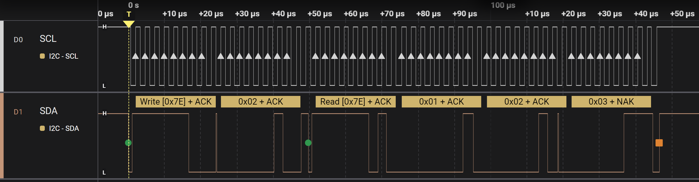
To achieve this goal, the following steps are required. Implement these steps in main.c when the interval has passed so the communication as seen above is transmitted at every interval.
- Wait as long as bus or controller is busy. Check the file lpi2c0_controller_interrupt.h for the available functions to do so.
- Clear all the status flags of the LPI2C. Check one of the example projects how to do so.
- Fill the transmit FIFO by putting in two words. Check the file lpi2c0_controller_interrupt.h for the available functions to do so.
- The first word consists of:
- CMD: Generate (repeated) Start on the I2C bus and transmit the address in DATA[7:0]
- DATA: slave address + write
- The second word consists of:
- CMD: Transmit the value in DATA[7:0]
- DATA: the variable rgb
- The first word consists of:
Check result 1
If implemented correctly, the target board shows the same RGB colour as the controller board does. However, the target board seems to freeze after several seconds. When resetting both boards, it will work again, but only for several seconds.
The reason for this behaviour is that the target sends three bytes for every byte it receives. The controller, however, never reads from the target. This means the transmit FIFO of the target will be full after several bytes. To solve this, the controller should read three bytes directly after every write of the rgb variable. This can be done with a repeated start condition. Add the following words in the transmit FIFO directly after putting in the previous words.
- Fill the transmit FIFO by putting in two more words.
- The first word consists of:
- CMD: Generate (repeated) Start on the I2C bus and transmit the address in DATA[7:0]
- DATA: slave address + read
- The second word consists of:
- CMD: Receive (DATA[7:0] + 1) bytes. DATA[7:0] is used as a byte counter.
- DATA: 2
- The first word consists of:
Check result 2
If implemented correctly, both boards will show the same LED colour. However, after a while, both will stop. The problem is now caused by the controller, because the receive FIFO is filled but never read.
In main, add the following code to make sure that the RXFIFO is read when data is available:
if(lpi2c0_rxcnt() >= 3)
{
    uint8_t data1 = lpi2c0_getword();
    uint8_t data2 = lpi2c0_getword();
    uint8_t data3 = lpi2c0_getword();

    // Check data from target
    if((data1 != 0x01) || (data2 != 0x02) || (data3 != 0x03))
    {
        // Data invalid
        GPIO3->PCOR = (1<<12);
        GPIO3->PSOR = (1<<13);
        GPIO3->PSOR = (1<<0);

        while(1)
        {}
    }
}
Verify that the communications is stable for a long period. Optionally, use a logic analyzer to visualize the result.
Assignment - I2C oled DMA driver
Resources: ese_shieldv3_examples\oled\dma
Goal
To know how to use the oled I2C display driver, understand how it is implemented using DMA, and its performance characteristics.
Hardware requirements
- FRDM-MCXA153 board
- Type-C USB cable
- 128x64 SSD1306 OLED display, available on Shield V3, or connect using four jumper wires
- Logic analyzer (optional)
Functional requirements
The application writes data to the oled display by using DMA.
Architecture
The Shield V3 shows an example of how to connect the hardware parts.
Oled display
The 128x64 dot matrix oled display used in this project uses the SSD1306 controller. The datasheet shows that several interfaces are supported (8-bit, 3-wire, 4-wire and I2C). This project uses the I2C interface with the oled display as a target and the MCXA153 as a controller.
Q1 Open the datasheet and find the target address of the SSD1306.
Why use DMA?
The oled display is a 128x64 dot matrix. Every dot is on or off and controlled by a single bit. This means that 128 x 64 = 8192 bits must be transmitted for a full screen update. As the I2C interface transmits bytes, this implies 1024 bytes must be transmitted. If I2C is configured in Fast mode, sending at 400 kbits/s, it will take approximately (1024 x (8+1)) x (1 / 400.000) = 23 ms to update the entire display. Due to this relative long duration, the CPU should be offloaded from this task by using DMA.
How to use DMA
A frame buffer of 1 kB (an unsigned char array of 1024 bytes) is declared in the microcontroller static RAM. Writing to the display actually updates this frame buffer in the microcontroller. Only by calling the function ssd1306_update(), this data is copied to a transmit buffer, a DMA transfer is started and the display is updated. This is depicted in the following sequence diagram.
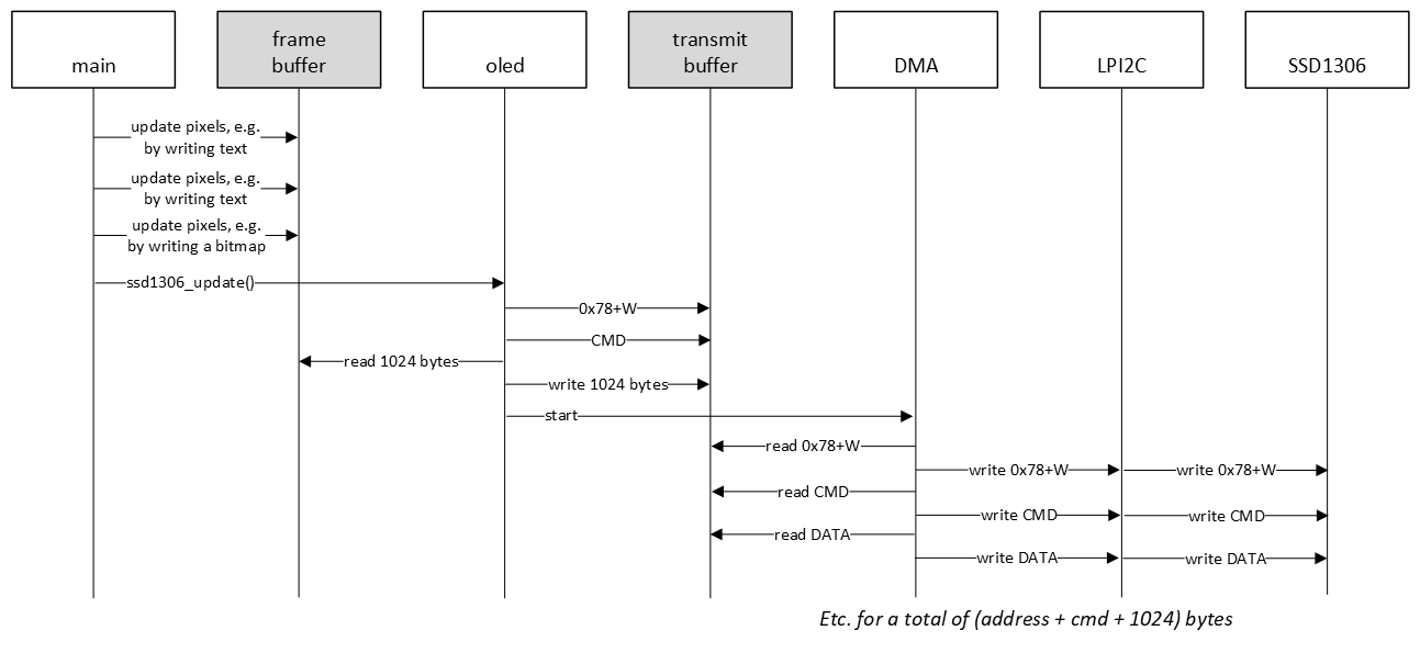
In all I2C examples so far, a hardware or software FIFO was used. In the sequence diagram above, a FIFO is not even mentioned. In this example, the 1024 byte frame buffer is actually first copied to a transmit buffer, and preceded by additional data, such as the target address and commands. This makes it easier to transmit all data with DMA, because the I2C controller requires 16-bit data (CMD and DATA). This driver is therefore double buffered. Another advantage of double buffering, is that if the main application updates the frame buffer, the transmit buffer will not be updated, unless the ssd1306_update() function is called.
One way to achieve frequent display updates is to use a timer and trigger a DMA transfer several times per second. This should not exceed approximately 40 times per second, because 40 times per second means an interval of 25 ms, which is barely enough to transmit all bytes in FAST mode.
SSD1306 configuration
The SSD1306 controller needs to be configured when it is powered on by sending the appropriate commands. Fortunately, the datasheet provides an example in terms of a software configuration flowchart. This is used as an inspiration for sending the initialisation commands when the application is started.
Q2 Browse the example project and find the array of initialisation commands.
The oled display contains a lot of features that can be controlled by sending the appropriate commands. An example is setting normal or inverse display.
Q3 What command needs to be transmitted in order to set inverse display?
Oled API
The SSD1306 driver provides the following API. All functions are documented in the source file.
void ssd1306_init(void);
void ssd1306_command(const uint8_t cmd);
void ssd1306_data(const uint8_t data);
void ssd1306_update(void);

void ssd1306_setfont(const char *f);
void ssd1306_setorientation(const uint8_t orientation);
void ssd1306_setinverse(const uint8_t inv);

void ssd1306_clearscreen(void);
void ssd1306_setcontrast(const uint8_t contrast);
void ssd1306_goto(const uint8_t x, const uint8_t y);
void ssd1306_setpixel(const uint8_t x, const uint8_t y, const pixel_value_t val);

void ssd1306_putchar(const char c);
void ssd1306_putstring(const uint8_t x, const uint8_t y, const char *str);

void ssd1306_drawline(uint8_t x0, uint8_t y0, uint8_t x1, uint8_t y1);
void ssd1306_drawbitmap(const unsigned char *bitmap);

void ssd1306_terminal(const char *str);
The main application demonstrates how to use several driver functions.
Finally, the following timing diagrams show the data transmissions. A debug pin was added and pulled low while the CPU was busy setting up the I2C DMA transfer. Instead of almost 25 ms, the CPU is busy for not even 1 ms, while the DMA controller transfers the data. And upon close inspection of the timing diagram, the majority of the 1 ms is spend in a delay that is required by the oled display between two transfers. This delay is implemented wit a for-loop, so timing depends on optimization settings. This could be tuned further, because the required delay is only 2 us.
SSD1306 DMA total:
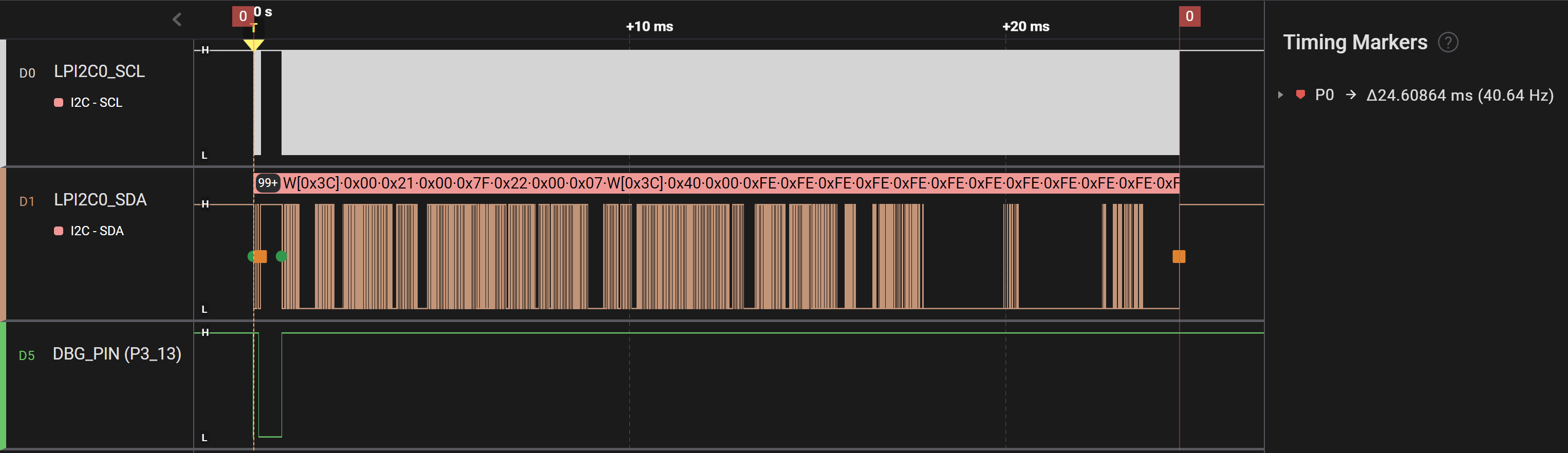
SSD1306 DMA detail:
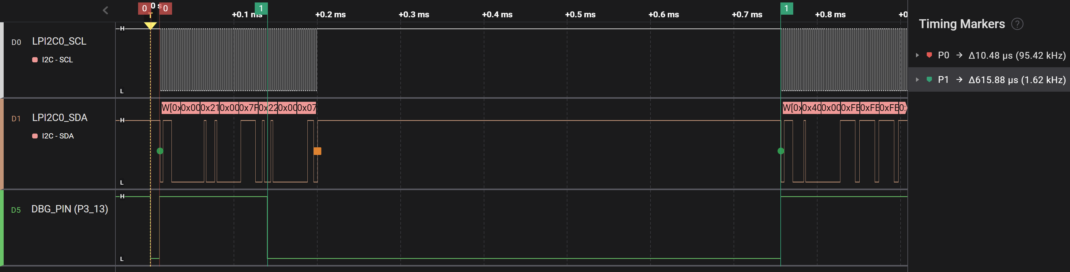
Assignment
Change the example application to display your name and student number. Familiarize yourself with the API by trying new fonts, drawing lines and/or drawing new bitmaps.
SPI - introduction
Resources: none
Goal
To understand the SPI communication protocol.
Communication protocol
The Serial Peripheral Interface (SPI) is a peer-to-peer interface. When compared to I2C, this means SPI doesn't need addressing. In order to address multiple devices a chip select is part of the interface. The following image depicts the physical connections:
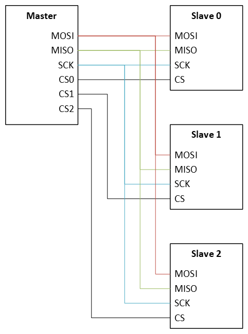
The abbreviations mean:
- MOSI: Master Out - Slave In
- MISO: Master In - Slave Out
- SCK: Serial clock
- CSn: Chip Select n
From a data path perspective, the following block diagram shows 8-bit frame size communication between a master and a slave. One can think of this as two shift registers that exchange data at the rate of the SCK signal. Usually, the MSB is transmitted first.
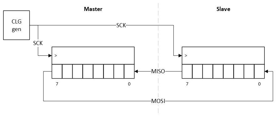
For example, if the master transmits 0xAA and the slave transmits 0x55, the following timing diagram will be generated:
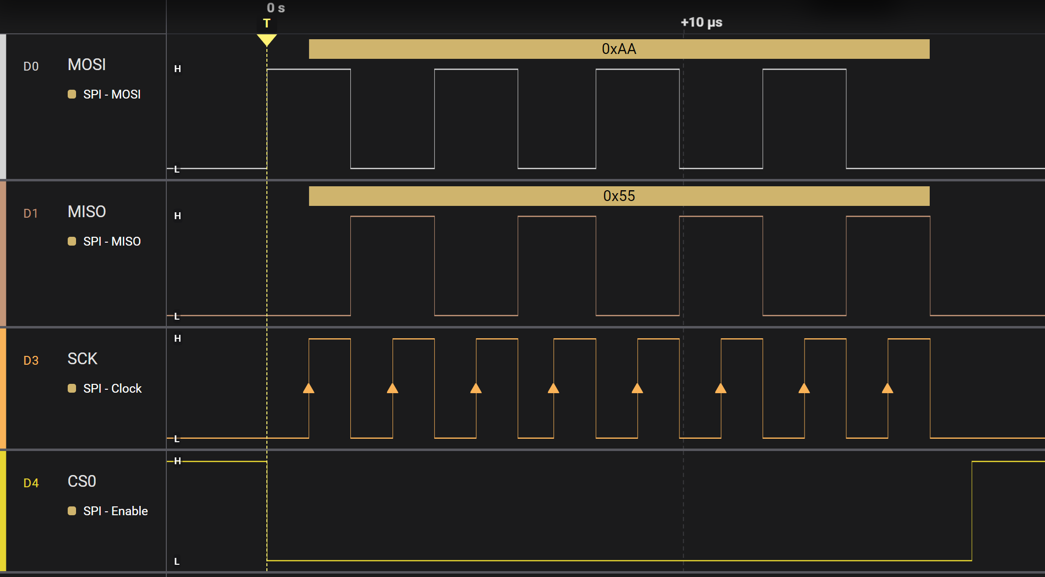
The timing diagram shows that:
- The CSn line is active low, meaning that a slave is selected by pulling the line low.
- On every rising edge of SCK, data from the master is latched by the slave and vice versa.
- At the end of the transfer the CSn line is pulled high.
Although this is a basic example, there are numerous configuration settings that might be applied. Examples are:
- Frame size
- Clock frequency
- Clock polarity
- Clock phase
- Chip select is active high instead of low
LPSPI Master and slave example - polling
Resources: ese_driver_examples\lpspi\master_slave_polling
Goal
To know how to configure the Low-Power SPI module for basic serial communication and use the LPSPI by polling bits in the status register.
Pin initialization
The MCXA153 microcontroller contains two Low-power SPI (LPSPI) modules: LPSPI0 and LPSPI1. In this example, LPSPI0 will be configured as a master and LPSPI1 as a slave. The following pins will be used:
| Master | Slave |
|---|---|
| P1_0/LPSPI0_SDO | P2_16/LPSPI1_SDI |
| P1_1/LPSPI0_SCK | P2_12/LPSPI1_SCK |
| P1_2/LPSPI0_SDI | P2_13/LPSPI1_SDO |
| P1_3/LPSPI0_PCS0 | P2_6/LPSPI1_PCS1 |
Part of the configuration code is as follows:
// Master
PORT1->PCR[0] = PORT_PCR_LK(1) | PORT_PCR_MUX(2) | PORT_PCR_IBE(1); // LPSPI0_SDO
PORT1->PCR[1] = PORT_PCR_LK(1) | PORT_PCR_MUX(2) | PORT_PCR_IBE(1); // LPSPI0_SCK
PORT1->PCR[2] = PORT_PCR_LK(1) | PORT_PCR_MUX(2) | PORT_PCR_IBE(1); // LPSPI0_SDI
PORT1->PCR[3] = PORT_PCR_LK(1) | PORT_PCR_MUX(2) | PORT_PCR_IBE(1); // LPSPI0_PCS0

// Slave
PORT2->PCR[6] = PORT_PCR_LK(1) | PORT_PCR_MUX(2) | PORT_PCR_IBE(1); // LPSPI1_PCS1
PORT2->PCR[12] = PORT_PCR_LK(1) | PORT_PCR_MUX(2) | PORT_PCR_IBE(1); // LPSPI1_SCK
PORT2->PCR[13] = PORT_PCR_LK(1) | PORT_PCR_MUX(2) | PORT_PCR_IBE(1); // LPSPI1_SDO
PORT2->PCR[16] = PORT_PCR_LK(1) | PORT_PCR_MUX(2) | PORT_PCR_IBE(1); // LPSPI1_SDI
If the SPI modules are clocked with the internal 12 MHz clock, and the LPSPI functional clock should be 1 MHz, the initial configuration for both SPI interfaces is almost the same:
// PCSCFG: [0] = PCS[3:2] configured for chip select function
// OUTCFG: [0] = Retain last value
// PINCFG: [00] =  SIN is used for input data; SOUT is used for output data
// MATCFG: [000] = Match is disabled
// PCSPOL: [0000] = Active low
// PARTIAL: [0] = n.a.
// NOSTALL: [0] = Disable stall transfers
// AUTOPCS: [0] = Disable automatic PCS
// SAMPLE: [0] = SCK edge
//
// MASTER: [1] = Master mode
LPSPI0->CFGR1 = LPSPI_CFGR1_MASTER(1);                 // <----- For master mode
//
// MASTER: [0] = Slave mode
LPSPI1->CFGR1 = 0;                                      // <----- For slave mode

// SCKPCS: [00000101] = SCK-to-PCS delay of (5+1) cycles
// PCSSCK: [00000101] = PCS-to-SCK delay of (5+1) cycles
// DBT: [00000000] = n.a.
// SCKDIV: [00000000] = n.a.
LPSPIn->CCR = 0x05050000;

// SCKSCK: [00000101] = SCK Inter-Frame delay of (5+1) cycles
// PCSPCS: [00000010] = PCS to PCS delay of (2 + 2 + 2) cycles
// SCKHLD: [00000101] = SCK hold of (5+1) cycles
// SCKSET: [00000101] = SCK setup of (5+1) cycles
LPSPIn->CCR1 = 0x05020505;

// RRF: [0] = No reset receive FIFO
// RTF: [0] = No reset transmit FIFO
// DBGEN: [0] = Disables LPSPI when the CPU is in debug mode
// RST: [0] = No software Reset
// MEN: [1] = Module enable
LPSPIn->CR = LPSPI_CR_MEN(1);
Hardware FIFOs
Similar to the LPI2C module, both LPSPI modules implement a 4-word receive and transmit hardware FIFO. So writing to the Transmit Data Register (TDR), actually pushes data into the transmit FIFO, as depicted in the following image.

Data exchange
When utilizing the entire 4-word FIFO, and transmitting 8-bit data frames, data is exchanged as depicted in the following sequence diagram:
Master                                                    Slave
  |       LPSPI0        LPSPI0  LPSPI1        LPSPI1        |
  |       RXFIFO        TXFIFO  TXFIFO        RXFIFO        |
  |          |             |       |             |          |
  |          |             |       |  write 0x10 |          |
  |          |             |       |<------------|----------+
  |          |             |       |  write 0x11 |          |
  |          |             |       |<------------|----------+
  |          |             |       |  write 0x12 |          |
  |          |             |       |<------------|----------+
  |          |             |       |  write 0x13 |          |
  |          | write 0x00  |       |<------------|----------+
  +----------|------------>|       |             |          |
  |          |    0x10     |       |     0x00    |          |
  |          |<------------+=======+------------>|          |
  |          | write 0x01  |       |             |          |
  +----------|------------>|       |             |          |
  |          | write 0x02  |       |             |          |
  +----------|------------>|       |             |          |
  |          | write 0x03  |       |             |          |
  +----------|------------>|       |             |          |
  |          |    0x11     |       |     0x01    |          |
  |          |<------------+=======+------------>|          |
  |          |    0x12     |       |     0x02    |          |
  |          |<------------+=======+------------>|          |
  |          |    0x13     |       |     0x03    |          |
  |          |<------------+=======+------------>|          |
  |          |             |       |             |read 0x01 |
  |          |             |       |             +--------->|
  |          |             |       |             |read 0x02 |
  |          |             |       |             +--------->|
  |          |             |       |             |read 0x03 |
  |          |             |       |             +--------->|
  |          |             |       |             |read 0x04 |
  | read 0x10|             |       |             +--------->|
  |<---------+             |       |             |          |
  | read 0x11|             |       |             |          |
  |<---------+             |       |             |          |
  | read 0x12|             |       |             |          |
  |<---------+             |       |             |          |
  | read 0x13|             |       |             |          |
  |<---------+             |       |             |          |
This means:
- The slave fills the TXFIFO.
- The master fills the TXFIFO. The initial write to the TXFIFO will also start the SPI transfer. While the transfer is ongoing, the rest of the data will be written to the TXFIFO.
- When all bytes are transferred, the slave reads the incoming data from the RXFIFO for verification.
- The master reads the incoming data from the RXFIFO for verification.
The following timing diagram shows the same data transfer:
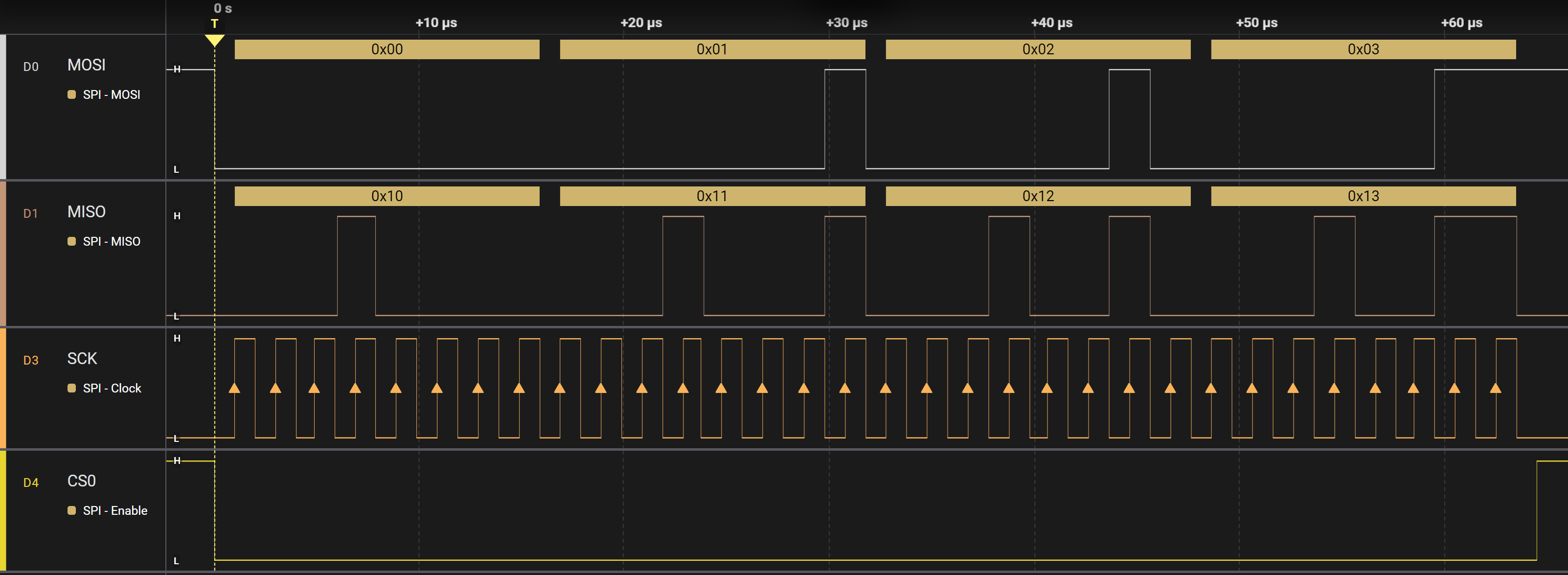
Notice that all signals, including the CS0 signal, are automatically generated by the LPSPI modules. This polling solution works well for small data sizes, but often more data needs to be transferred. For this purpose interrupts or DMA can be used.
Assignment
None.
LPSPI Master and slave example - interrupt
Resources: ese_driver_examples\lpspi\master_slave_interrupt
Goal
To know how to configure the Low-Power SPI module for basic serial communication and use the SPI with interrupts.
Circular buffer
Similar to using an interrupt driven UART and I2C, transmitted and received data needs to be stored temporarily. Fortunately, the MCXA153A microcontroller features a LPSPI module with a four word hardware FIFO (see LPSPI - polling for more info). However, if more than four words need to be temporary stored, a software solution should be made. Similar to the UART and I2C, a circular buffer is a suitable data structure.
API
The API for both master and slave will be as follows:
// Initialize the LPSPI module in master mode
void lpspi0_master_init(void);

// Writes n bytes from buffer to a software FIFO and initiates the first SPI transfer to the slave
void lpspi0_master_tx(uint8_t *buffer, const uint32_t n);

// Reads n bytes from a software FIFO into buffer
void lpspi0_master_rx_read(uint8_t *buffer, const uint32_t n);

// Initialize the LPSPI module in slave mode
void lpspi1_slave_init(void);

// Writes n bytes from buffer to a software FIFO to be transmitted to the master
void lpspi1_slave_rx_start(uint8_t *buffer, const uint32_t n);

// Reads n bytes from a software FIFO into buffer
void lpspi1_slave_rx_read(uint8_t *buffer, const uint32_t n);
This API is similar to the LPSPI - polling example. However, due to the software FIFO, the number of data items is restricted by the size of the software FIFO and not the 4-word hardware FIFO.
Assignment
Change the example so it transmits the ASCII characters of your name from master to slave. The slave sends back your student number, followed by 0x00 for any remaining characters. Use a logic analyzer to visualize the MOSI, MISO, SCK and CS0 signals. Also change the clock settings so the SCK frequency is equal to 125 kHz. Tip: only the master clock configuration needs to be updated.
Assignment - Shift register
Resources: ese_shieldv3_examples\shiftregister\lpspi
Goal
To practice with the modules discussed so far.
Hardware requirements
- FRDM-MCXA153 board
- HC595 shift register (and 8 LEDs for visualisation of the outputs), such as available on Shield V3 or Mikroe-1824 add-on board
- Type-C USB cable
- Logic analyzer (optional)
Note. When using the Mikroe add-on board, different pins must be used!
Functional requirements
The application controls the 8 outputs of a shift register. The shift register is controlled with an SPI interface.
Architecture
The Shield V3 shows an example of how to connect the hardware parts. Notice that the MISO pin and QH' pin are not connected.
API
In order to create the functional requirements, the following API functions are prepared.
/*!
 * \brief Initializes the HC595 pins
 *
 * Resources:
 * - GPIO output | P3_1
 * - LPSPI1
 *
 * Pin P3_1 is configured as an GPIO output pin. The pin is toggled from low to
 * high in order to trigger the SRCLR pin of the HC595. It furthermore
 * configures LPSPI1 as a master by calling the lpspi1_master_init() function.
 */
void hc595_init(void);

/*!
 * \brief Writes a single byte to the shift register
 *
 * Uses the lpspi1_master_tx() function for transmitting the data.
 *
 * \param[in] data Data item to transmit
 */
void hc595_write(uint8_t data);
Implement these functions. In main, use these functions to create an LED chaser. The behaviour is depicted in the following sequence diagram:
                                               lpspi1           shift
     main              hc595                   txfifo  gpio3     reg.
     ---                ---                     ---     ---      ---
      |                  |                       |       |        |
      | hc595_init       |                       |       |        |
      +----------------->|                       |       |        |
      |                  | init P3_1             |       |        |
      |                  +-----------------------|------>|        |
      |                  | P3_1 = SRCLR = 0      |       |        |
      |                  +-----------------------|------>|------->|
      |                  | P3_1 = SRCLR = 1      |       |        |
      |                  +-----------------------|------>|------->|
      |                  | lpspi1_master_init    |       |        |
      |                  +---------------------->|       |        |
      | hc595_write 0x01 |                       |       |        |
      +----------------->|                       |       |        |
      |                  | lpspi1_master_tx 0x01 |       |        |
   +->|                  +---------------------->|       |  0x01  |
   |  |                  |                       +-------|------->|
   +--+                  |                       |       |        |
 125ms|                  |                       |       |        |
      | hc595_write 0x02 |                       |       |        |
      +----------------->|                       |       |        |
      |                  | lpspi1_master_tx 0x02 |       |        |
   +->|                  +---------------------->|       |  0x02  |
   |  |                  |                       +-------|------->|
   +--+                  |                       |       |        |
 125ms|                  |                       |       |        |
      | hc595_write 0x04 |                       |       |        |
      +----------------->|                       |       |        |
      |                  | lpspi1_master_tx 0x04 |       |        |
   +->|                  +---------------------->|       |  0x04  |
   |  |                  |                       +-------|------->|
   +--+                  |                       |       |        |
 125ms|                  |                       |       |        |
TIP: Use the SysTick timer to create a millisecond timer for the 125 ms delay in main.
Assignment - EEPROM
Resources: ese_shieldv3_examples\eeprom\lpspi
Goal
To practice with the modules discussed so far.
Hardware requirements
- FRDM-MCXA153 board
- M950x0 EEPROM, available on Shield V3 or Mikroe-1200 add-on board
- Type-C USB cable
- Logic analyzer (optional)
Note. When using the Mikroe add-on board, different pins must be used and different instructions are applicable! Carefully study the datasheet of the used EEPROM on the add-on board.
Functional requirements
The application reads and writes from an external EEPROM. This is done through an SPI interface.
Architecture
The Shield V3 shows an example of how to connect the hardware parts.
EEPROM
EEPROM chips are devices that are controlled by sending instructions. One can think of an EEPROM, or any external device for that matter, as a microcontroller with very specific functions. It has internal registers that can be read and/or written through one of it's interfaces. In this case, the used interface is SPI.
The EEPROM datasheet shows a table with instructions. Some of these instructions are:
| Instruction | Description | Format bin | Format hex |
|---|---|---|---|
| WREN | Write enable | 0000 X110 | 0x06 |
| WRDI | Write disable | 0000 X100 | 0x04 |
| RDSR | Read Status register | 0000 X101 | 0x05 |
| WRSR | Write Status register | 0000 X001 | 0x01 |
| READ | Read EEPROM memory | 0000 0011 | 0x03 |
| WRITE | Write EEPROM memory | 0000 0010 | 0x02 |
In order to fully understand the devices features, one should carefully read the datasheet. Particular important are the reset values of the internal registers.
As an example, the following sequence diagram shows how the microcontroller can send the WREN instruction.
   LPSPI1             LPSPI1
   TXFIFO   EEPROM    RXFIFO
     ---      ---      ---
      |        |        |
      |  0x06  |        |
      +------->+        |
      |        |        |
The output of the EEPROM (MISO) is high impedance, so the value read by LPSPI1 should be ignored (RXMASK enabled).
A timing diagram with similar information is shown in the datasheet.
Here is another example for reading the RDSR instruction. Now the values read by LPSPI1 should not be ignored, however only the second values in the RXFIFO is actually considered a valid value.
   LPSPI1             LPSPI1
   TXFIFO   EEPROM    RXFIFO
     ---      ---      ---
      |        |        |
      |  0x05  |  0x00  |
      +------->+------->|
      |  0x00  |  0xF0  |
      +------->+------->|
      |        |        |
In this example:
- The LPSPI1 sends the RDSR (0x05) instruction. The EEPROM MISO pin is in high impedance state so 0x00 will be read by LPSPI1. This incoming byte should be discarded.
- The LPSPI1 sends dummy data (0x00 in the sequence diagram), and the EEPROM transmits the content of it's status register (0xF0), which can be read by LPSPI1.
A timing diagram showing similar information is shown in the datasheet.
API
In order to create the functional requirements, several API functions have already been prepared:
void lpspi1_wait_busy(void);
void lpspi1_tx(uint8_t *buffer, const uint32_t n, uint32_t rxmsk);
void lpspi1_rx_read(uint8_t *buffer, const uint32_t n);
void eeprom_init(void);
These functions can be used to implement the following API functions:
/*!
 * \brief Returns the content of the status register
 *
 * This functions sends the RDSR (0x05) instruction. After that, dummy data is
 * transmitted in order to receive the content of the 8-bit status register.
 *
 * \Return Content of the status register
 */
uint8_t eeprom_rdsr(void);

/*!
 * \brief Returns true if a write is in progress
 *
 * This functions reads the status register and returns true if the Write in
 * progress bit is set
 *
 * \Return true  WIP bit is set
 *         false WIP bit is not set
 */
bool eeprom_wip(void);

/*!
 * \brief Sets Write enable true or false
 *
 * Sends the write enable (WREN) or write disable (WRDI) to the EEPROM. Data
 * from the EEPROM is ignored.
 *
 * \param[in] wel true  WREN instruction is send
 *                false WRDI instruction is send
 */
void eeprom_we(bool wel);

/*!
 * \brief Reads n bytes starting at address
 *
 * This function fills the TXFIFO with the appropriate instruction and address.
 * A transfer is then initiated by calling the lpspi_tx() function as follows:
 * lpspi1_tx(NULL, 0, 0);
 * This will start the transfer of the instruction, address and n dummy bytes.
 * The result is copied into buffer by using the lpspi1_rx_read() function.
 *
 * \param[in]  address EEPROM start address
 * \param[out] buffer  pointer to store the data
 * \param[in]  n       number of bytes
 */
void eeprom_read(uint8_t address, uint8_t *buffer, const uint32_t n);

/*!
 * \brief Writes n bytes starting at address
 *
 * This function fills the TXFIFO with the appropriate instruction and address.
 * A transfer is then initiated by calling the lpspi_tx() function with the.
 *
 * \param[in]  address EEPROM start address
 * \param[in]  buffer  pointer to get the data
 * \param[in]  n       number of bytes
 */
void eeprom_write(uint8_t address, uint8_t *buffer, const uint32_t n);
Implement these functions. In main, these functions are already called to read/write from the EEPROM.
Some tips:
- While working on these functions, use a logic analyzer to visualize the data.
- When reading from the EEPROM, by default, all memory locations read 0xFF. Reading n bytes from the EEPROM means that the READ instruction and the address (see datasheet) must be transmitted first. This is depicted in the following sequence diagram.
   LPSPI1                              LPSPI1
   TXFIFO              EEPROM          RXFIFO
     ---                ---             ---
      |                  |               |
      | 0x03: READ inst. |  0x00: dummy  |
      +----------------->+-------------->|
      |                  |               |
      | 0x00: address    |  0x00: dummy  |
      +----------------->+-------------->|
      |                  |               |
      | 0x00: dummy      |  0xFF: data 1 |
      +----------------->+-------------->|
      |                  |               |
      | 0x00: dummy      |  0xFF: data 2 |
      +----------------->+-------------->|
      .                  .               .
      .                  .               .
      | 0x00: dummy      |  0xFF: data n |
      +----------------->+-------------->|
      |                  |               |
As an example: here is a timing diagram of reading the status register and four bytes from memory:
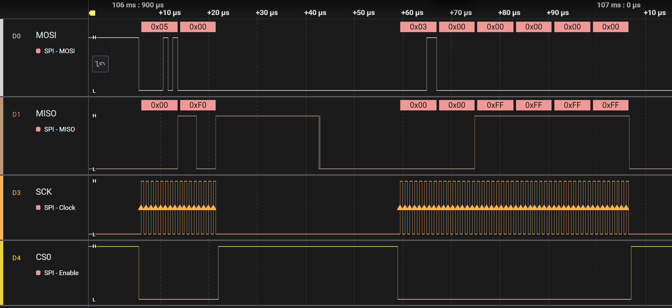
- Before writing to the EEPROM in main, make sure that writing is enabled with the eeprom_we() function. After writing is done, wait while a write is in progress with the eeprom_wip() function.
Hardfault
Resources: ese_general_examples\basics\hardfault
Goal
Use the debugger and the hardfault handler to solve the hardfault errors in this project.
Hardfaults
A hardfault exception is a special type of exception generated by the Cortex-M core. It is generally speaking not possible to recover from a hardfault exception. Examples of hardfault exceptions for the MCXA153 microcontrollers are:
- Accessing a peripheral register when the clock to that peripheral has not been enabled.
- Accessing a peripheral register when it is not released from reset.
- Unaligned memory access – for example trying to read or write a 32-bit integer from an address that is not a multiple of four.
When a hardfault exception occurs, the Cortex-M core will generate a hardfault interrupt. The function prototype of this ISR is:
void HardFault_Handler(void);
The debugger can be used to verify if a hardfault has occurred, for example by setting a breakpoint in the hardfault ISR. As it is not possible to recover from a hardfault, hardfault ISRs often implement an endless loop.
Final assignment
The project contains three mistakes. Use the debugger as follows to solve the three mistakes:
- Build the project
- Start the debugger
- Step through the code until the hardfault ISR is executed
- What instruction caused the hardfault ISR to execute?
- Stop the debugger
- Solve the problem
Repeat the above steps until all problems are solved. When all problems are solved correctly, the green RGB LED blinks.
Cyclic scheduler
Resources: ese_general_examples\advanced\cyclic_scheduler
Goal
To know how to implement a cyclic executive with interrupts scheduler.
Introduction
In microcontroller applications the right thing should happen at the right time. Or at least before a given deadline. But what if the project becomes a large collection of functional modules? What options do we have to process the incoming events, while making sure the application remains responsive?
Several options exists that are beyond the scope of this course content. One option is to use a finite state-machine. Another option is a real-time operating system such as FreeRTOS. This course discusses yet another option: a cyclic executive with interrupt scheduler.
Cyclic executive with interrupt scheduler
There is a single CPU core in the MCXA153 microcontroller that can execute machine instructions. If multiple tasks need to be executed, the CPU time for executing instruction should be divided somehow between these tasks. This is called scheduling.
In a cyclic executive scheduler, all tasks take turn one after the other. This is depicted in the following image:
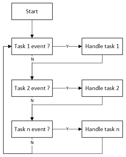
Two considerations for handling tasks are:
- Tasks are only executed if an event needs to be handled.
- Execution time of a task is as short as possible. This means, for example no delays. Instead of using delays, create a new event that is started in a task handler and finished when the timeout event occurs.
Tasks are checked and handled in a fixed order, hence the name cyclic executive. Events can be generated when handling a task, but more likely by interrupt handlers. In this type of scheduling, interrupts will always have priority over the task handlers!
When there are no events, the CPU will spend it's time doing nothing but checking if events occurred. In a fully interrupt driven application, the CPU can thus be put in sleep mode to reduce power consumption.
Example
The scheduler is implemented with if-statements in a endless while-loop in main. For example:
// -----------------------------------------------------------------------------
// Local variables
// -----------------------------------------------------------------------------
static volatile uint32_t ms = 0;
static uint32_t timeout = 0xFFFFFFFF;
static uint8_t color = 0;

// -----------------------------------------------------------------------------
// Main application
// -----------------------------------------------------------------------------
int main(void)
{
    gpio_input_init();
    gpio_output_init();
    lpuart0_init(9600);

    // Generate an interrupt every 1 ms
    SysTick_Config(48000);

    printf("Cyclic executive with interrupts scheduler");
    printf(" - %s\r\n", TARGETSTR);
    printf("Build %s %s\r\n", __DATE__, __TIME__);

    while(1)
    {
        // --------------------------------------------------------------------
        // Switch pressed event?
        if(gpio_input_sw3_pressed())
        {
            printf("[%08lu] event: switch pressed\r\n", ms);

            timeout = ms + 3000;

            const uint32_t lut[3] =  {(1<<13), (1<<12), (1<<0)};

            GPIO3->PCOR = lut[color];
        }

        // --------------------------------------------------------------------
        // Timeout event?
        if(ms >= timeout)
        {
            printf("[%08lu] event: timeout\r\n", ms);

            timeout = 0xFFFFFFFF;

            GPIO3->PSOR = (1<<0);
            GPIO3->PSOR = (1<<12);
            GPIO3->PSOR = (1<<13);
        }

        // --------------------------------------------------------------------
        // Incoming data event?
        if(lpuart0_rxcnt() > 0)
        {
            int data = lpuart0_getchar();

            printf("[%08lu] event: incoming data \'%c\'\r\n", ms, data);

            if(data == ' ')
            {
                printf("[%08lu] color updated\r\n", ms);
                color = (color == 2) ? 0 : color + 1;
            }
        }
    }
}
In the example, three events are handled:
- Switch pressed event
- Timeout event
- Incoming data event
If one of the events occurs, it is logged via serial with printf() and visualized on the RGB LED.
A major benefit of this design is that it is fairly easy to add the handling of more events.
Assignment
Add an event that is triggered every second. Reuse the ms counter for this purpose. Verify the result by printing a log message via serial.
C to assembly
Resources: ese_general_examples\advanced\c_to_assembly
Goal
To know the programmers model of the ARM Cortex-M processor. To know what a machine instruction is and know how to read several simple instructions written in assembly. To know the memory regions and what decisions a compiler makes when assigning a variable to a memory region. To know what the AAPCS is and what it tells about passing arguments and the return value of functions. Use type and class qualifiers to instruct the compiler to treat declarations different from default.
Cortex-M architecture
An ARM Cortex-M microcontroller is a machine that can be programmed to execute instructions. These instructions are often located in ROM memory, but can also be located in RAM.
Example machine instruction are:
- the addition of two numbers (ADD)
- the multiplication of two numbers (MUL)
- comparing two numbers (CMP)
- bitwise and-ing two numbers (AND)
- bitwise inverting a number (MVN)
- etc.
Two main architectures exist for the implementation of such machines:
- Load/store architecture, where machine instructions can access core registers only. This means:
- Load data into the core
- Process the data within the core
- Store the data back in memory or register
- Register/memory architecture, where machine instructions can access both memory and core registers.
ARM Cortex-M microcontrollers are load/store architectures.
Machine instructions
The MCXA153 microcontroller features an ARM Cortex-M33 CPU. This CPU is based on the Armv8-M architecture. The supported instructions by this machine are described in the Armv8-M Architecture Reference Manual.
An example is the MUL instruction. The reference manual shows that it is implemented by two variants, called T1 and T2. T1 is a 16-bit instruction and T2 is a 32-bit instruction. The description shows how the instruction translates to 1's and 0's that will be stored in memory. However, for several bit-fields the 1's and 0's depend on the selected register:
- Rn: source register in the core. n is is a three or four bit value, depending on the variant.
- Rm: source register in the core. m is is a three or four bit value, depending on the variant.
- Rd: destination register in the core. d is is a three or four bit value, depending on the variant.
Programmers model
The available core registers are described in Armv8-M Architecture Reference Manual. This is known as the programmers model and depicted in the following overview:
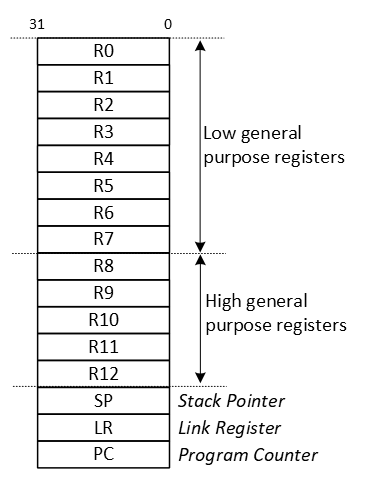
As shown, there are sixteen 32-bit core registers.
Let's take a closer look at variant T2 of the MUL instruction:
Now, given de following instruction:
MUL R7, R0, R1
In this instruction:
- Rd=R7
- Rn=R0
- Rm=R1
This will yield the following instruction that will be stored in memory:
                        Rn            Rd            Rm
| 11111 | 0110 | 000 | 0000 | 1111 | 0111 | 0000 | 0001 |
This is equal to 0xFB00F701 in hexadecimal.
Conclusion: the core registers are used as sources and destination for the machine instructions. Machine instructions and their operands need to be loaded into the CPU before execution, hence the load/store architecture.
Assembly
Instead of having to write such binary or hexadecimal codes, the assembly language was developed. The general form of an instruction written in assembly is:
<operation> <operand1> <operand2> <operand3>
There may be fewer operands. The first operand typically is the destination register, the others are source registers.
As an example, the multiplication instruction as mentioned above in assembly is:
MUL R7, R0, R1
An assembler is a tool that is normally installed as part of the IDE and translates assembly instructions to machine instructions. Assembly instructions are often located in .s files or in inline assembly directly in .c files. An example of inline assembly is
for(uint32_t i=0; i<1000; i++)
{
    // NOP is the No Operation instruction. It has no operands and is used to wait one CPU clock cycle.
    __asm("nop");
}
Special registers
As can be seen in the programmers model, several special registers exist. These are the program counter (PC), the link register (LR), and the stack pointer (SP). The purpose of these registers is explained in more detail later, after taking a look at the memories that are available in the microcontroller.
Memories
An ARM Cortex-M microcontroller features a 32-bit memory map. This means that 2^32 = 4 GB of bytes can be addressed. The memory map of the MCXA153 microcontroller is as follows:
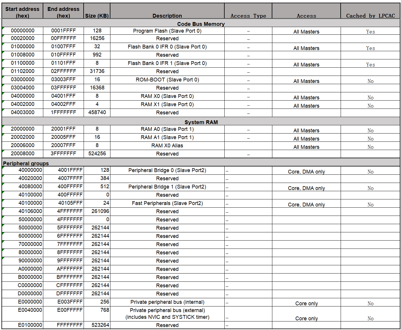
The memory map shows which addresses are in use to access flash, RAM, peripheral registers and core registers.
The available RAM memory, which is 32 kB (8 + 16 + 8, starting from address 0x20000000) for the MCXA153, is used in three ways:
-
For static R/W data
These variables exist from program start to program end and are typically global variables. Static in this context means a static memory address, not a static value.
-
For automatic R/W data
These variables exist from function start to function end and are typically variables declared within a function. Automatic in this context means that the memory address is assigned during runtime. It is unknown at compile time. The memory region called stack is used for this purpose, which will be explained in more detail later.
-
For temporary R/W data
These variables exist from explicit allocation to explicit deallocation. This is done with functions such as malloc() and free(). The allocated memory remains allocated, even when a function returns. The memory region called heap is used for this purpose, which will be explained in more detail later.
Why these different options? Most often, the amount of RAM in a microcontroller is limited. So compilers try to reuse the available RAM us much as possible.
The following image shows two typical RAM layouts. The image was inspired by this blog.
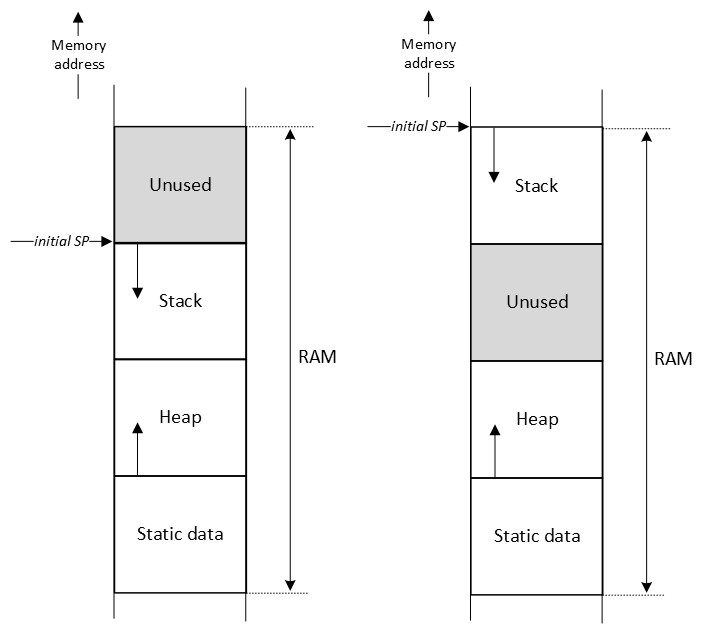
The size of the Static data region is known at compile time. The size of the Heap and Stack regions are configurable in the IDE, for example in a scatter (.sct) file. If malloc() is not used in the application, the heap size can be set to zero. All microcontroller applications use a stack. To determine the size of the stack of you application, this blog is a must read. Notice that library functions, such as printf(), and interrupt handlers, also use the stack.
The stack is a LIFO data structure to temporarily store data. The top of the stack is recorded by the stack pointer (SP in programmers model). As can be seen in the image, in a Cortex-M microcontroller, the stack grows from a high memory address to a low memory address. If the size of the stack is not managed properly, chances are that other regions are overwritten when the stack increases. There is no hardware mechanism that checks, for example, that the SP is equal to an address that is used for the heap region.
As mentioned, the stack is used to store automatic variables. In addition, the stack is also used for storing other 'housekeeping' data, such as the value of core registers. If a function is called, and in this function register R7 must be used, the content of R7 can be saved on the stack at the start of the function, R7 can be used for the duration of the function, and at the end of the function, the value can be restored. This is achieved by using the PUSH and POP operations as follows:
                     multiply:       // 'multiply' is called a label. It is translated into a
                                     // memory address by the linker. This memory address,
                                     // holds the first instruction of this function (entry
                                     // point).

0x00000214 B480      PUSH  {R7}      // R7 is used in this function, but it's value should be
                                     // restored after this function is done. Therefore, save it
                                     // on the stack.

0x00000216 FB00F701  MUL   R7,R0,R1  // Multiply R0 and R1 and store the result in R7.
0x0000021A 4638      MOV   R0,R7     // R0 should contain the multiplied result, so move it.

0x0000021C BC80      POP   {R7}      // Restore the value of R7

0x0000021E 4770      BX    LR        // Return from function
The example above shows in the first column the address where the instruction is stored in memory and in the second column the instruction in hexadecimal notation. The address of the instruction that will be executed next by the CPU is stored in the program counter (PC in programmers model). After the instruction is executed, the PC is automatically increased by the size of the instruction (2 or 4 bytes).
In case a function is executed, the CPU needs to remember where it came from. In other words, what is the address of the next instruction? This address is stored in the link register (LR in programmers model) and used when returning from a function as shown in the last instruction in the example above. It simply means that the PC will get the value of the LR and operation continues where it left off.
As there is a single LR in the CPU core, you might wonder what happens with the LR if inside a function another function is called? In that case, the LR will first be stored on the stack and at the end of the function be restored.
Type and class qualifiers
The C programming language contains keywords that can be used to tell the compiler to treat declarations different from default.
-
const
These variables are only read and not written. They can be located in ROM instead of RAM.
const char *str = "This string is located in ROM memory\n";
-
static
These variables are always assigned a fixed memory address and will be placed in the static memory region. Even when declared in a function. An advantage of this is the fact that the value is not reset between function invocations and the scope of the variable is that particular function.
static uint32_t global_cnt = 0;

void pulse_counter(void)
{
    // This variable is newly created on the stack each time this function is called
    uint32_t local_cnt = 0;

    // This variable is created one time in static data section
    static uint32_t static_cnt = 0;

    // What is the value of these variables when this functions has been called 10 times?
    local_cnt++;
    static_cnt++;
    global_cnt++;
}
-
volatile
These variables can change outside normal program flow and should never be optimized by the compiler. Examples are variables shared between main and an ISR. Or peripheral registers. Not being optimized means that the compiler should implement a load-store operation for each access to this variable, instead of keeping a copy in a core register.
static volatile bool switch_pressed_flag = false;
Q1 Given the following example application. For each variable:
- Will it be located in RAM or ROM?
- If in RAM, will it be located in the stack, heap, or static region?
int var01 = 0;
unsigned char var02 = 0;
char var03[32] = {0};

static int var04 = 0;
static unsigned char var05 = 0;
static char var06[32] = {0};

volatile int var07 = 0;
volatile unsigned char var08 = 0;
volatile char var09[32] = {0};

const int var10 = 0;
const unsigned char var11 = 0;
const char var12[32] = {0};

int func(int a, int b)
{
    int var13 = 0;
    unsigned char var14 = 0;
    char var15[32] = {0};

    static int var16 = 0;
    static unsigned char var17 = 0;
    static char var18[32] = {0};

    volatile int var19 = 0;
    volatile unsigned char var20 = 0;
    volatile char var21[32] = {0};

    const int var22 = 0;
    const unsigned char var23 = 0;
    const char var24[32] = {0};

    return a + b;
}

int main(void)
{
    int var25 = 0;
    unsigned char var26 = 0;
    char var27[32] = {0};

    static int var28 = 0;
    static unsigned char var29 = 0;
    static char var30[32] = {0};

    volatile int var31 = 0;
    volatile unsigned char var32 = 0;
    volatile char var33[32] = {0};

    const int var34 = 0;
    const unsigned char var35 = 0;
    const char var36[32] = {0};

    var25 = func(1,2);

    while(1)
    {}
}
AAPCS
One important topic not discussed so far is the way arguments are passed to and from functions. One can think of several options, such as the stack, the core registers, or a dedicated section of the static RAM. In order to standardize these options, ARM came up with the Procedure Call Standard for Arm Architecture AAPCS.
For passing arguments, the following basic rules apply:
- Process arguments in order they appear in source code
- Round size up to a multiple of four bytes
- Use core registers R0 to R3, align doubles to even registers
- Use stack for remaining arguments, align doubles to even addresses
- Call the function (LR is saved and PC gets the value of the first instruction of that function)
For returning a value from a function, the following basic rules apply:
-
Returning a fundamental data type (e.g. int, char, pointer, etc.)
- 1-4 bytes: R0
- 8 bytes: R0-R1
- 16 bytes: R0-R3
-
Returning a composite data types
- 1-4 bytes: R0
- all other sizes: stack
If the stack is used, the caller function allocates space for the return value and passes the pointer to that space to the function.
Notice that the core registers are preferred, because this is faster when compared to the stack.
Compiler differences
Compilers are used to translate C code into machine instructions. Although code is generated for the same machine, you should assume that different compilers will generate different instructions. This is even true when using another version of the same compiler. Or when changing compiler settings, such as optimization.
Two compilers that are often used for ARM Cortex-M processors are ArmClang and GCC. To provide a basic idea of the differences, the generated machine instructions generated for the function sum() is compared. The function is implemented and called as follows:
int32_t sum(int32_t a, int32_t b)
{
    return a + b;
}

int main(void)
{
    int32_t s = 0;
    int32_t m = 0;

    s = sum(1, 2);

    m = mul(1, 2);

    while(1)
    {}
}
- Compiler: AC6 (ArmClang V6.21) - Optimization: -O0
    67: {                                  // As per AAPCS: arguments a and b are in R0 and R1
0x00000590 B082      SUB      sp,sp,#8     // Creates space for 8 bytes (for 2 32-bit registers) on the stack
0x00000592 9001      STR      r0,[sp,#4]   // Store argument a on the stack, 4 address relative from the SP
0x00000594 9100      STR      r1,[sp,#0]   // Store argument b on the stack, 0 address relative from the SP
    68:     return a + b;
0x00000596 9801      LDR      r0,[sp,#4]   // Load argument a from the stack in R0, 4 address relative from the SP
0x00000598 9900      LDR      r1,[sp,#0]   // Load argument b from the stack in R1, 0 address relative from the SP
0x0000059A 4408      ADD      r0,r0,r1     // Execute operation: R0 = R0 + R1. Result in R0 as per AAPCS
0x0000059C B002      ADD      sp,sp,#8     // Restore stack space for 8 bytes
0x0000059E 4770      BX       lr           // Branch to where the application came from
- Compiler: GCC (Arm GNU Toolchain 12.2.Rel1 (Build arm-12.24)) 12.2.1 20221205 - Optimization: -O0
67        {                                // As per AAPCS: arguments a and b are in R0 and R1
          sum:
00004a6e:            push    {r7}          // Save R7 on the stack
00004a70:            sub     sp, #12       // Creates space for 12 bytes (for 3 32-bit registers) on the stack
00004a72:            add     r7, sp, #0    // Save the value of SP in R7
00004a74:            str     r0, [r7, #4]  // Store argument a on the stack, 4 address relative from R7
00004a76:            str     r1, [r7, #0]  // Store argument b on the stack, 0 address relative from R7
68                     return a + b;
00004a78:            ldr     r2, [r7, #4]  // Load argument a from the stack in R2, 4 address relative from R7
00004a7a:            ldr     r3, [r7, #0]  // Load argument b from the stack in R3, 0 address relative from R7
00004a7c:            add     r3, r2        // Execute operation: R3 = R3 + R2
69        }
00004a7e:            mov     r0, r3        // Move the value in R3 to R0 as per AAPCS
00004a80:            adds    r7, #12       // Calculate restored stack space for 12 bytes
00004a82:            mov     sp, r7        // Restore stack space
00004a84:            pop     {r7}          // Restore R7
00004a86:            bx      lr            // Branch to where the application came from
- Compiler: AC6 (ArmClang V6.21) - Optimization: -O3
The function is never called, because the result is not used in main.
- Compiler: GCC (Arm GNU Toolchain 12.2.Rel1 (Build arm-12.24)) 12.2.1 20221205 - Optimization: -O3
The function is never called, because the result is not used in main.
From a functional point of view, the two compilers with the same settings produce code that behaves exactly the same. They both calculate the sum of the two numbers in R0 and R1 and return the result in R0. The machine instructions to produce this result are, however, quite different.
Q2 Why is there no need to store the LR on the stack in the sum() function?
Example - Extra
The following application starts in the function main(). Instead of the C instructions, the assembly instructions are given in the first column. For each instruction, the updated value of several registers is presented after the instruction is executed. Examine the table and make sure you understand why a particular value is assigned to a register.
Note. This example is created with:
- Compiler: AC6 (ArmClang V6.21) - Optimization: -O0
- Debugger: Keil MDK-ARM
| Executed instruction | PC | LR | SP | R1 | R0 | Note |
|---|---|---|---|---|---|---|
| 0x00000588 | 0x00000527 | 0x20005FF0 | 0x40091824 | 0x00000589 | Initial situation when main is started | |
| PUSH | 0x0000058A | 0x20005FE8 | R7 and LR are pushed on the stack, so the SP decrements by 8-bytes | |||
| SUB sp,sp,#0x18 | 0x0000058C | 0x20005FD0 | Space for 24 (0x18) more bytes allocated on the stack | |||
| MOVS r0,#0 | 0x0000058E | 0x00000000 | Move the value 0 into R0 (# means immediate) | |||
| STR r0,[sp,#8] | 0x00000590 | Store the value in R0 8 places relative from the SP | ||||
| STR r0,[sp,#0x14] | 0x00000592 | Store the value in R0 20 places relative from the SP | ||||
| STR r0,[sp,#0x10] | 0x00000594 | Store the value in R0 16 places relative from the SP | ||||
| MOVS r0,#1 | 0x00000596 | 0x00000001 | Move the value 1 into R0 | |||
| STR r1,[sp,#4] | 0x00000598 | Store the value in R1 4 places relative from the SP | ||||
| MOVS r1,#2 | 0x0000059A | 0x00000002 | Move the value 2 into R1 | |||
| STR r1,[sp,#0] | 0x0000059C | Store the value in R1 0 places relative from the SP | ||||
| BL sum (0x000005E0) | 0x000005E0 | 0x000005A1 | Branch to sum() function. The PC is set to the address of the first instruction of sum(). The LR is set to the address of the next instruction in main | |||
| SUB sp,sp,8 | 0x000005E2 | 0x20005FC8 | Space for 8 more bytes allocated on the stack | |||
| STR r0,[sp,#4] | 0x000005E4 | Store the value in R0 4 places relative from the SP | ||||
| STR r1,[sp,#0] | 0x000005E6 | Store the value in R1 0 places relative from the SP | ||||
| LDR r0,[sp,#4] | 0x000005E8 | Load the value in R0 that is located 4 places relative from the SP | ||||
| LDR r1,[sp,#0] | 0x000005EA | Load the value in R1 that is located 0 places relative from the SP | ||||
| ADD r0,r0,r1 | 0x000005EC | 0x00000003 | R0 = R0 + R1 | |||
| ADD sp,sp,#8 | 0x000005EE | 0x20005FD0 | Space for 8 bytes restored from the stack | |||
| BX lr | 0x000005A0 | Branch to the address saved in the LR | ||||
| STR r0,[sp,#0x14] | 0x000005A2 | Store the value in R0 20 places relative from the SP | ||||
| Etc. |
Assignment
Q3 What is the purpose of the PC?
Q4 What is the purpose of the LR?
Q5 What is the purpose of the SP?
Given the following function prototype:
int func(int a, int b);
Q6 According the AAPCS, how are the arguments a and b passed?
Q7 And also according AAPCS, how is the value returned?
Q8 What is the purpose of the PUSH and POP instructions?
Q9 Is an automatic variable stored in the stack, heap or static data?
Q10 Why is it called an automatic variable?
Given the following declaration of a global variable:
static int var = 0;
Q11 What does static in this context mean?
Q12 What is the heap?
Q13 What is the purpose of the type qualifier const?
Q14 In a Cortex-M application, how is the size of the static data, stack and heap managed?
Given the following code example:
typedef struct
{
    uint32_t level;
    char name[36];
} test_t;

void func1(test_t test);
void func2(test_t *test);
Q15 What is the difference in terms of memory usage for func1() and func2()?