LPI2C Controller example - polling
Resources: ese_driver_examples\lpi2c\controller_polling_p3t1755
Goal
To know how to configure the Low-Power I2C module for basic serial communication and use the LPI2C by polling bits in the status register.
Pin initialization
The FRDM-MCXA153 board contains the P3T1755 digital temperature sensor. The board schematic page 7 shows the following pin connections:
- P0_16: LPI2C0_SDA
- P0_17: LPI2C0_SCL
The initialization of these required modules is as follows:
// Set clock source
// MUX: [010] = FRO_HF_DIV
MRCC0->MRCC_LPI2C0_CLKSEL = MRCC_MRCC_LPI2C0_CLKSEL_MUX(2);

// HALT: [0] = Divider clock is running
// RESET: [0] = Divider isn't reset
// DIV: [0000] = divider value = (DIV+1) = 1
MRCC0->MRCC_LPI2C0_CLKDIV = 0;

// Enable modules and leave others unchanged
// LPI2C0: [1] = Peripheral clock is enabled
// PORT0: [1] = Peripheral clock is enabled
MRCC0->MRCC_GLB_CC0_SET = MRCC_MRCC_GLB_CC0_LPI2C0(1);
MRCC0->MRCC_GLB_CC0_SET = MRCC_MRCC_GLB_CC0_PORT0(1);

// Release modules from reset and leave others unchanged
// LPI2C0: [1] = Peripheral is released from reset
// PORT0: [1] = Peripheral is released from reset
MRCC0->MRCC_GLB_RST0_SET = MRCC_MRCC_GLB_RST0_LPI2C0(1);
MRCC0->MRCC_GLB_RST0_SET = MRCC_MRCC_GLB_RST0_PORT0(1);

// Configure P0_16 and P0_17
// LK : [1] = Locks this PCR
// INV: [0] = Does not invert
// IBE: [1] = Digital Input Buffer Enable, otherwise pin is used for analog
//            functions
// MUX: [0010] = Alternative 2
// DSE: [0] = low drive strength is configured on the corresponding pin,
//            if the pin is configured as a digital output
// ODE: [0] = Disables
// SRE: [0] = Fast
// PE:  [1] = Enables
// PS:  [1] = Enables internal pullup resistor
PORT0->PCR[16] = PORT_PCR_LK(1) | PORT_PCR_MUX(2) | PORT_PCR_PE(1) |
    PORT_PCR_PS(1) | PORT_PCR_ODE(1) | PORT_PCR_IBE(1); // LPI2C0_SDA
PORT0->PCR[17] = PORT_PCR_LK(1) | PORT_PCR_MUX(2) | PORT_PCR_PE(1) |
    PORT_PCR_PS(1) | PORT_PCR_ODE(1) | PORT_PCR_IBE(1); // LPI2C0_SCL
I2C controller initialization
It takes the following steps to configure the I2C module as a controller, as described in the reference manual paragraph 36.5:
- Configure Controller Configuration 0 (MCFGR0) Controller Configuration 3 (MCFGR3) as required by the application.
- Configure Controller Clock Configuration 0 (MCCR0) and Controller Clock Configuration 1 (MCCR1) to satisfy the timing requirements of the I2C mode supported by the application.
- Enable controller interrupts and DMA requests as required by the application.
- Enable the LPI2C controller by writing 1 to MCR[MEN].
Step 3. is not needed, because this is a polling example. The other steps are explained in more detail in the following sections.
1. & 2. Configure Controller and clock Configuration
The I2C specification describes several modes of operation, such as Standard, Fast, Fast+, and HS. The P3T1755 supports Fast mode (see section 12 Dynamic characteristics).
Configuring a controller in a specific mode requires the configuration of several configuration registers called MCFGRn and MCCRn. The reference manual paragraph 36.6 shows a convenient table with example timing configurations for several modes. The following settings apply for Fast mode with a 48 MHz clock frequency (which was selected in the previous step with FRO_HF_DIV as the clock source).
// I2C timing parameters to setup the following specifications (see
// paragraph 36.6 (NXP, 2024)):
// I2C mode: FAST
// Clock frequency: 48 MHz
// I2C baud rate: 400 kbits/s
LPI2C0->MCFGR1 = LPI2C_MCFGR1_PRESCALE(0);
LPI2C0->MCFGR2 = LPI2C_MCFGR2_FILTSDA(1) | LPI2C_MCFGR2_FILTSCL(1);

LPI2C0->MCCR0 = LPI2C_MCCR0_DATAVD(0x0F) | LPI2C_MCCR0_SETHOLD(0x1D) |
    LPI2C_MCCR0_CLKHI(0x35) | LPI2C_MCCR0_CLKLO(0x3E);
4. Enable the LPI2C controller by writing 1 to MCR[MEN]
// MEN: [1] = Controller Enable
// Rest unchanged
LPI2C0->MCR |= LPI2C_MCR_MEN(1);
Writing data
The transmission of I2C data is not as 'simple' when compared to a UART. Where a UART module automatically adds a start-bit, stop-bit(s), etc. for each transmitted data item, this is not possible for I2C data because of the afore mentioned protocol. The embedded programmer must explicitly state what part of the protocol must be initiated by the hardware.
Generally speaking, writing a single byte to a single register in a target device in a polling implementation takes the following protocol steps:
- Wait while the I2C bus is busy.
- Clear all LPI2C status flags.
- Generate a START condition and transmit target address + w.
- Wait for it to complete.
- Transmit the register address to write to.
- Wait for it to complete.
- Transmit the data.
- Wait for it to complete.
- Generate a STOP condition.
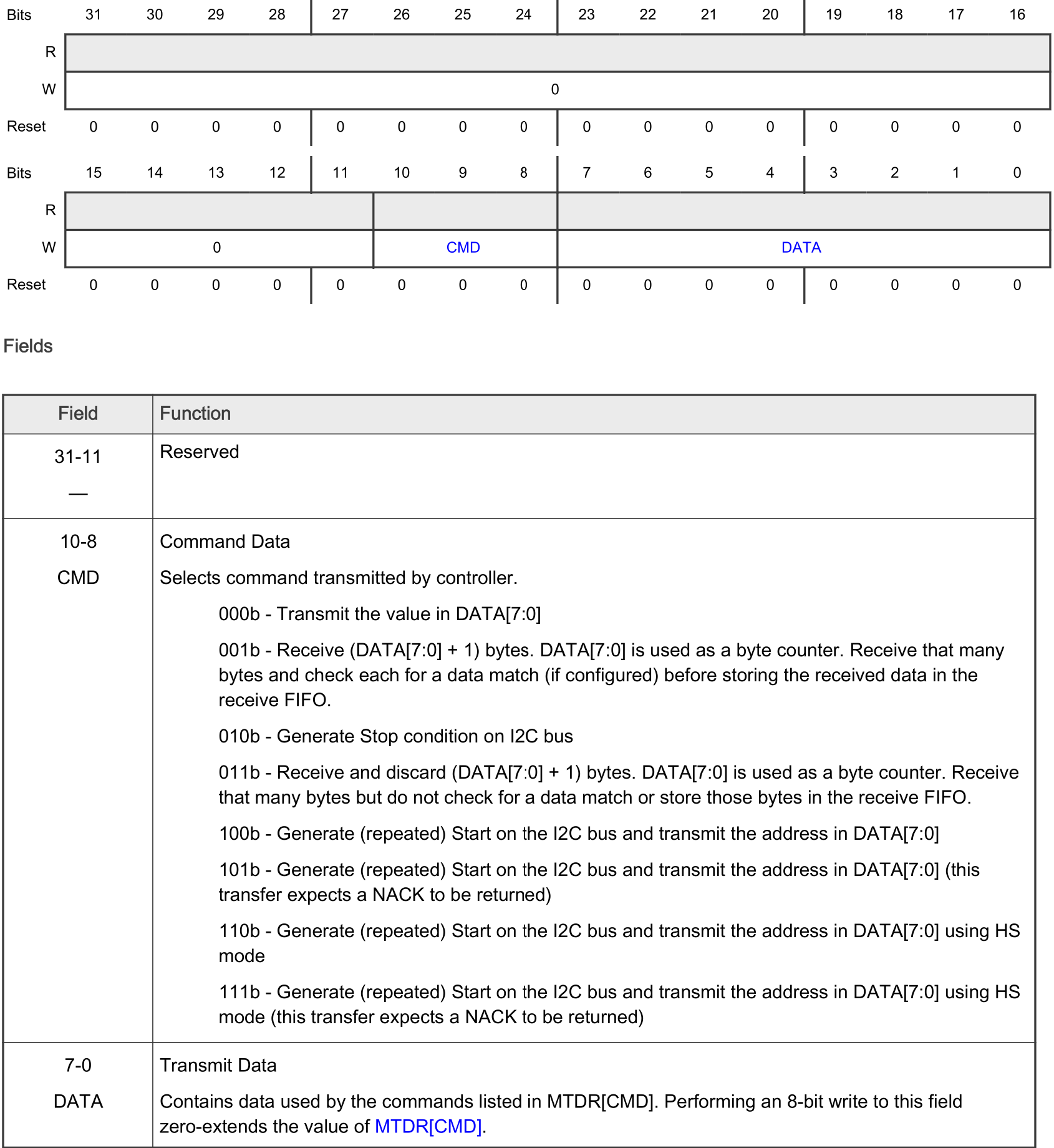
In order to do this in the MCXA153 microcontroller, the LPI2C module has a register that is used for both I2C commands and, if applicable, the associated data. The command (CMD) consists of three bits and the DATA of eight bits:

These 11 bits share a single register called MTDR. The reference manual paragraph 36.7 describes this register in detail:
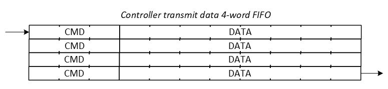
The steps 3, 5 7 and 9 are all writes to the MTDR register. In a polling implementation, the firmware must wait for the operation to complete after each write. However, the MCXA153 provides a 4 word hardware FIFO. This means the firmware can write four times to the MTDR register without having to wait for the operation to complete. This FIFO mechanism is depicted as follows:
The following function is a generic function for writing data, that takes advantage of the FIFO mechanism:
void lpi2c0_write(const uint8_t dev_address, const uint8_t reg, uint8_t *p,
    const uint8_t len)
{
    // Wait as long as bus or controller is busy
    lpi2c0_wait_busy();

    // Clear all status flags
    LPI2C0->MSR = LPI2C_MSR_STF_MASK | LPI2C_MSR_DMF_MASK |
        LPI2C_MSR_PLTF_MASK | LPI2C_MSR_FEF_MASK | LPI2C_MSR_ALF_MASK |
        LPI2C_MSR_NDF_MASK | LPI2C_MSR_SDF_MASK | LPI2C_MSR_EPF_MASK;

    // Note. Four words can be written to the MTDR register, because of the
    //       four word transmit FIFO (8-bit transmit data + 3-bit command).
    //       If more must be written, use the function lpi2c0_txfifo_full()
    //       after four words to wait until the FIFO is not full anymore.

    // Command: 100b - Generate (repeated) Start on the I2C bus and transmit
    //          the address in DATA[7:0]
    // Data   : Slave address + w
    LPI2C0->MTDR = LPI2C_MTDR_CMD(0b100) | LPI2C_MTDR_DATA(dev_address);

    // Command: 000b - Transmit the value in DATA[7:0]
    // Data   : index low byte
    LPI2C0->MTDR = LPI2C_MTDR_CMD(0b000) | LPI2C_MTDR_DATA(reg);

    for(uint32_t i=0; i<len; ++i)
    {
        // Wait while transmit fifo full
        while(lpi2c0_txfifo_full())
        {}

        // Command: 000b - Transmit the value in DATA[7:0]
        // Data   : data
        LPI2C0->MTDR = LPI2C_MTDR_CMD(0b000) | LPI2C_MTDR_DATA(p[i]);
    }

    // Wait while transmit fifo full
    while(lpi2c0_txfifo_full())
    {}

    // Command: 010b - Generate Stop condition on I2C bus
    // Data   : n.a.
    LPI2C0->MTDR = LPI2C_MTDR_CMD(0b010);
}
And a PT3T1755 specific function to set the configuration register is as follows:
void p3t1755_set_configuration_reg(uint8_t val)
{
    // Device address: 0b1001000 (P3T1755)
    // Pointer byte: 0b00000001 (Configuration register)
    // Send one byte: val
    lpi2c0_write(0b1001000, 0b00000001, &val, 1);
}
Reading data
Generally speaking, reading a single byte from a single register in a target device in a polling implementation takes the following protocol steps:
- Wait while the I2C bus is busy.
- Clear all LPI2C status flags.
- Generate a START condition and transmit target address + w.
- Wait for it to complete.
- Transmit the register address to read from.
- Wait for it to complete.
- Generate a repeated START condition and transmit target address + r.
- Wait for it to complete.
- Set the number of bytes to receive to 1.
- Wait for incoming data.
- Read the incoming data.
- Generate a STOP condition.
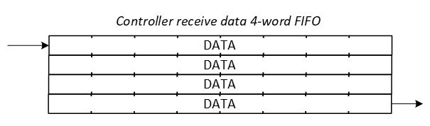
The controller also implements a four word FIFO for the reception of data:
The following function is a generic function for reading data, that takes advantage of the FIFO mechanism:
void lpi2c0_read(const uint8_t dev_address, const uint8_t reg, uint8_t *p,
    const uint8_t len)
{
    // Wait as long as bus or controller is busy
    lpi2c0_wait_busy();

    // Clear all status flags
    LPI2C0->MSR = LPI2C_MSR_STF_MASK | LPI2C_MSR_DMF_MASK |
        LPI2C_MSR_PLTF_MASK | LPI2C_MSR_FEF_MASK | LPI2C_MSR_ALF_MASK |
        LPI2C_MSR_NDF_MASK | LPI2C_MSR_SDF_MASK | LPI2C_MSR_EPF_MASK;

    // Note. Four words can be written to the MTDR register, because of the
    //       four word transmit FIFO (8-bit transmit data + 3-bit command).
    //       If more must be written, use the function lpi2c0_txfifo_full()
    //       after four words to wait until the FIFO is not full anymore.

    // Command: 100b - Generate (repeated) Start on the I2C bus and transmit
    //          the address in DATA[7:0]
    // Data   : Slave address + w
    LPI2C0->MTDR = LPI2C_MTDR_CMD(0b100) | LPI2C_MTDR_DATA(dev_address << 1);

    // Command: 000b - Transmit the value in DATA[7:0]
    // Data   : index low byte
    LPI2C0->MTDR = LPI2C_MTDR_CMD(0b000) | LPI2C_MTDR_DATA(reg);

    // Command: 100b - Generate (repeated) Start on the I2C bus and transmit
    //          the address in DATA[7:0]
    // Data   : Slave address + r
    LPI2C0->MTDR = LPI2C_MTDR_CMD(0b100) | LPI2C_MTDR_DATA((dev_address << 1) | 1);

    // Command: 001b - Receive (DATA[7:0] + 1) bytes. DATA[7:0] is used as a
    //          byte counter.
    // Data   : count
    LPI2C0->MTDR = LPI2C_MTDR_CMD(0b001) | LPI2C_MTDR_DATA(len - 1);

    // Receive the data
    for(uint32_t i=0; i<len; ++i)
    {
        // Wait while the RXFIFO is empty
        while(lpi2c0_rxfifo_empty())
        {}

        // Read the data
        p[i] = (uint8_t)LPI2C0->MRDR;
    }

    // Wait while transmit fifo full
    while(lpi2c0_txfifo_full())
    {}

    // Command: 010b - Generate Stop condition on I2C bus
    // Data   : n.a.
    LPI2C0->MTDR = LPI2C_MTDR_CMD(0b010);
}
Reading the P3T1755 configuration register is thus done as follows:
uint8_t p3t1755_get_configuration_reg(void)
{
    uint8_t data = 0;

    // Device address: 0b1001000 (P3T1755)
    // Pointer byte: 0b00000001 (Configuration register)
    lpi2c0_read(0b1001000, 0b00000001, &data, 1);

    return data;
}
Notes
If polling is used, be careful that the FIFOs are 4 words. It is not possible to write more without data corruption. If more than four words need to be written to the FIFO, the firmware must wait until the FIFO is not full any more. The function lpi2c0_txfifo_full() can be used for this purpose, which checks the number of items in the MTDR FIFO by reading the MFSR register.
Another option would be to store all CMD+DATA in an array and use interrupts for the transmission. This is discussed in the next topic.
Assignment
None.