LPSPI Master and slave example - polling
Resources: ese_driver_examples\lpspi\master_slave_polling
Goal
To know how to configure the Low-Power SPI module for basic serial communication and use the LPSPI by polling bits in the status register.
Pin initialization
The MCXA153 microcontroller contains two Low-power SPI (LPSPI) modules: LPSPI0 and LPSPI1. In this example, LPSPI0 will be configured as a master and LPSPI1 as a slave. The following pins will be used:
| Master | Slave |
|---|---|
| P1_0/LPSPI0_SDO | P2_16/LPSPI1_SDI |
| P1_1/LPSPI0_SCK | P2_12/LPSPI1_SCK |
| P1_2/LPSPI0_SDI | P2_13/LPSPI1_SDO |
| P1_3/LPSPI0_PCS0 | P2_6/LPSPI1_PCS1 |
Part of the configuration code is as follows:
// Master
PORT1->PCR[0] = PORT_PCR_LK(1) | PORT_PCR_MUX(2) | PORT_PCR_IBE(1); // LPSPI0_SDO
PORT1->PCR[1] = PORT_PCR_LK(1) | PORT_PCR_MUX(2) | PORT_PCR_IBE(1); // LPSPI0_SCK
PORT1->PCR[2] = PORT_PCR_LK(1) | PORT_PCR_MUX(2) | PORT_PCR_IBE(1); // LPSPI0_SDI
PORT1->PCR[3] = PORT_PCR_LK(1) | PORT_PCR_MUX(2) | PORT_PCR_IBE(1); // LPSPI0_PCS0

// Slave
PORT2->PCR[6] = PORT_PCR_LK(1) | PORT_PCR_MUX(2) | PORT_PCR_IBE(1); // LPSPI1_PCS1
PORT2->PCR[12] = PORT_PCR_LK(1) | PORT_PCR_MUX(2) | PORT_PCR_IBE(1); // LPSPI1_SCK
PORT2->PCR[13] = PORT_PCR_LK(1) | PORT_PCR_MUX(2) | PORT_PCR_IBE(1); // LPSPI1_SDO
PORT2->PCR[16] = PORT_PCR_LK(1) | PORT_PCR_MUX(2) | PORT_PCR_IBE(1); // LPSPI1_SDI
If the SPI modules are clocked with the internal 12 MHz clock, and the LPSPI functional clock should be 1 MHz, the initial configuration for both SPI interfaces is almost the same:
// PCSCFG: [0] = PCS[3:2] configured for chip select function
// OUTCFG: [0] = Retain last value
// PINCFG: [00] =  SIN is used for input data; SOUT is used for output data
// MATCFG: [000] = Match is disabled
// PCSPOL: [0000] = Active low
// PARTIAL: [0] = n.a.
// NOSTALL: [0] = Disable stall transfers
// AUTOPCS: [0] = Disable automatic PCS
// SAMPLE: [0] = SCK edge
//
// MASTER: [1] = Master mode
LPSPI0->CFGR1 = LPSPI_CFGR1_MASTER(1);                 // <----- For master mode
//
// MASTER: [0] = Slave mode
LPSPI1->CFGR1 = 0;                                      // <----- For slave mode

// SCKPCS: [00000101] = SCK-to-PCS delay of (5+1) cycles
// PCSSCK: [00000101] = PCS-to-SCK delay of (5+1) cycles
// DBT: [00000000] = n.a.
// SCKDIV: [00000000] = n.a.
LPSPIn->CCR = 0x05050000;

// SCKSCK: [00000101] = SCK Inter-Frame delay of (5+1) cycles
// PCSPCS: [00000010] = PCS to PCS delay of (2 + 2 + 2) cycles
// SCKHLD: [00000101] = SCK hold of (5+1) cycles
// SCKSET: [00000101] = SCK setup of (5+1) cycles
LPSPIn->CCR1 = 0x05020505;

// RRF: [0] = No reset receive FIFO
// RTF: [0] = No reset transmit FIFO
// DBGEN: [0] = Disables LPSPI when the CPU is in debug mode
// RST: [0] = No software Reset
// MEN: [1] = Module enable
LPSPIn->CR = LPSPI_CR_MEN(1);
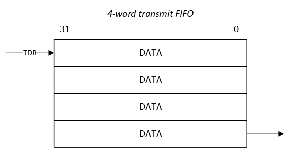
Hardware FIFOs
Similar to the LPI2C module, both LPSPI modules implement a 4-word receive and transmit hardware FIFO. So writing to the Transmit Data Register (TDR), actually pushes data into the transmit FIFO, as depicted in the following image.
Data exchange
When utilizing the entire 4-word FIFO, and transmitting 8-bit data frames, data is exchanged as depicted in the following sequence diagram:
Master                                                    Slave
  |       LPSPI0        LPSPI0  LPSPI1        LPSPI1        |
  |       RXFIFO        TXFIFO  TXFIFO        RXFIFO        |
  |          |             |       |             |          |
  |          |             |       |  write 0x10 |          |
  |          |             |       |<------------|----------+
  |          |             |       |  write 0x11 |          |
  |          |             |       |<------------|----------+
  |          |             |       |  write 0x12 |          |
  |          |             |       |<------------|----------+
  |          |             |       |  write 0x13 |          |
  |          | write 0x00  |       |<------------|----------+
  +----------|------------>|       |             |          |
  |          |    0x10     |       |     0x00    |          |
  |          |<------------+=======+------------>|          |
  |          | write 0x01  |       |             |          |
  +----------|------------>|       |             |          |
  |          | write 0x02  |       |             |          |
  +----------|------------>|       |             |          |
  |          | write 0x03  |       |             |          |
  +----------|------------>|       |             |          |
  |          |    0x11     |       |     0x01    |          |
  |          |<------------+=======+------------>|          |
  |          |    0x12     |       |     0x02    |          |
  |          |<------------+=======+------------>|          |
  |          |    0x13     |       |     0x03    |          |
  |          |<------------+=======+------------>|          |
  |          |             |       |             |read 0x01 |
  |          |             |       |             +--------->|
  |          |             |       |             |read 0x02 |
  |          |             |       |             +--------->|
  |          |             |       |             |read 0x03 |
  |          |             |       |             +--------->|
  |          |             |       |             |read 0x04 |
  | read 0x10|             |       |             +--------->|
  |<---------+             |       |             |          |
  | read 0x11|             |       |             |          |
  |<---------+             |       |             |          |
  | read 0x12|             |       |             |          |
  |<---------+             |       |             |          |
  | read 0x13|             |       |             |          |
  |<---------+             |       |             |          |
This means:
- The slave fills the TXFIFO.
- The master fills the TXFIFO. The initial write to the TXFIFO will also start the SPI transfer. While the transfer is ongoing, the rest of the data will be written to the TXFIFO.
- When all bytes are transferred, the slave reads the incoming data from the RXFIFO for verification.
- The master reads the incoming data from the RXFIFO for verification.
The following timing diagram shows the same data transfer:
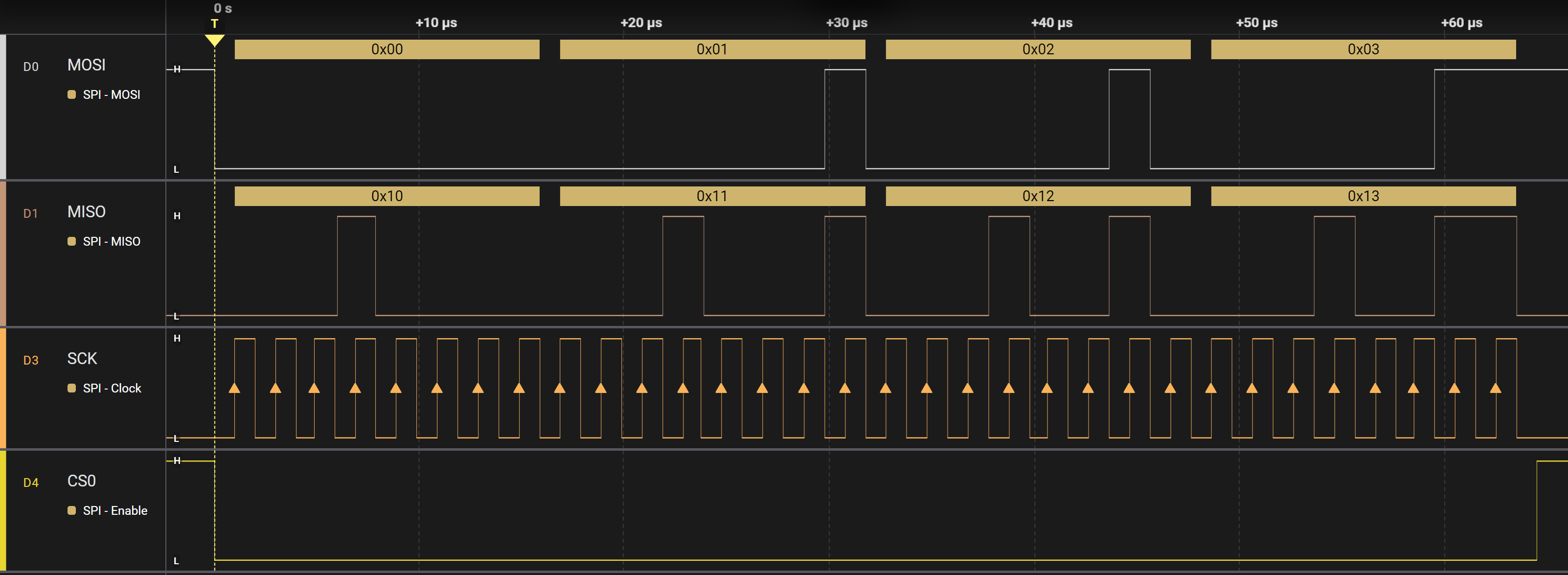
Notice that all signals, including the CS0 signal, are automatically generated by the LPSPI modules. This polling solution works well for small data sizes, but often more data needs to be transferred. For this purpose interrupts or DMA can be used.
Assignment
None.