GPIO output
Resources: ese_driver_examples\gpio\output
Goal
Know how to initialize and control a digital output pin with the GPIO module.
RGB LED - Which pin to use?
The FRDM-MCXA153 board contains an RGB LED that can be controlled by the user. Before being able to control the RGB LED, the physical connection on the FRDM-MCXA153 board must be verified. Checking the board schematic page 7 shows the following pin connections:
- LED_RED: PORT3 pin 12 (P3_12)
- LED_GREEN: PORT3 pin 13 (P3_13)
- LED_BLUE: PORT3 pin 0 (P3_0)
PORTn modules provide support for pin control functions. This microcontroller features four PORT modules: PORT0 to PORT3. Each PORT module is capable of controlling 32 pins (provided that a pin is available on the particular microcontroller package).
Initialization
GPIO modules can be used to control the logic state of a microcontroller pin. However, a pin must first be configured for the GPIO function. This is done in the PORT module. Using P3_13 as an example, it takes the following steps to configure the pin for GPIO:
- Enable the PORT3 and GPIO3 modules in the Module Reset and Clock Control (MRCC) module.
- Initialize P3_13 for GPIO function in the PORT3 module.
- Initialize P3_13 for output function in the GPIO3 module.
These steps are explained in more detail in the following sections.
1. Enable the PORT3 and GPIO3 modules
The MRCC module must be used to enable other modules, such as PORT3 and GPIO3. How this is done is described in the reference manual paragraph 14.3.
// Before a module can be used, its clocks must be enabled (CC != 00) and it
// must be released from reset (MRCC_GLB_RST [peripherals name] = 1). If a
// module is not released from reset (MRCC_GLB_RST [peripherals name] = 0),
// an attempt to access a register within that module is terminated with a
// bus error.
This description translates to the following C instructions for the GPIO3 and PORT3 modules:
// Enable modules and leave others unchanged
// GPIO3: [1] = Peripheral clock is enabled
// PORT3: [1] = Peripheral clock is enabled
MRCC0->MRCC_GLB_CC1 |= MRCC_MRCC_GLB_CC1_GPIO3(1);
MRCC0->MRCC_GLB_CC1 |= MRCC_MRCC_GLB_CC1_PORT3(1);

// Release modules from reset and leave others unchanged
// GPIO3: [1] = Peripheral is released from reset
// PORT3: [1] = Peripheral is released from reset
MRCC0->MRCC_GLB_RST1 |= MRCC_MRCC_GLB_RST1_GPIO3(1);
MRCC0->MRCC_GLB_RST1 |= MRCC_MRCC_GLB_RST1_PORT3(1);
The use of defines such as MRCC_MRCC_GLB_CC1_PORT3(1) for bit fields makes the code very readable and portable. The naming convention for such defines is as follows:
MODULE_REGISTER_BITFIELD(x)
Want to know how this define works and what other defines are available? Read this!
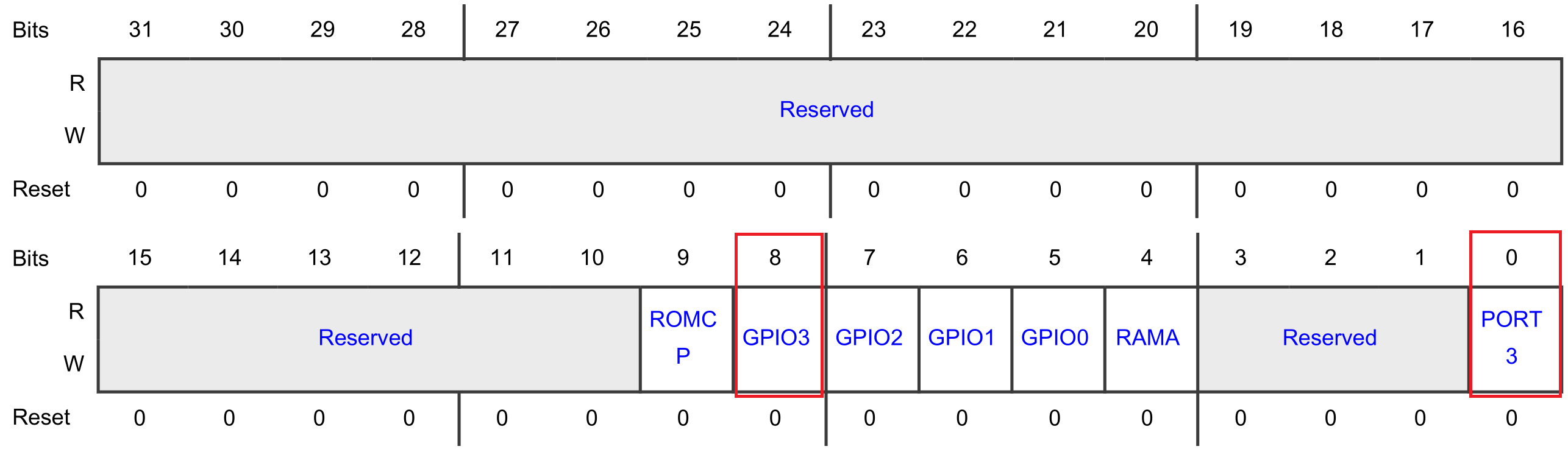
These instructions set bit 0 and bit 8, because according the MRCC_GLB_CC1 and MRCC_GLB_RST register diagrams:
- PORT3 is bit position 0
- GPIO3 is bit position 8
So, alternatively, the following instructions could have been used:
// Enable modules and leave others unchanged
// GPIO3: [1] = Peripheral clock is enabled
// PORT3: [1] = Peripheral clock is enabled
MRCC0->MRCC_GLB_CC1 |= (1<<0);
MRCC0->MRCC_GLB_CC1 |= (1<<8);

// Release modules from reset and leave others unchanged
// GPIO3: [1] = Peripheral is released from reset
// PORT3: [1] = Peripheral is released from reset
MRCC0->MRCC_GLB_RST1 |= (1<<0);
MRCC0->MRCC_GLB_RST1 |= (1<<8);
2. Initialize P3_13 for GPIO function
The PORT module must be used to configure the function for a pin. How this is done is described in the reference manual paragraph 11.4.
// 1. Initialize the pin functions:
//    -  Initialize single pin functions by writing appropriate values to
//       PCRn
//    -  Initialize multiple pins (up to 16) with the same configuration by
//       writing appropriate values to Global Pin Control Low (GPCLR) or
//       Global Pin Control High (GPCHR).
// 2. Lock the configuration for a given pin, by writing 1 to PCRn [LK], so
//    that it cannot be changed until the next reset.
There is a PCR register for each and every pin. The reference manual describes the PCR registers in detail, for example PCR10-PCR13:
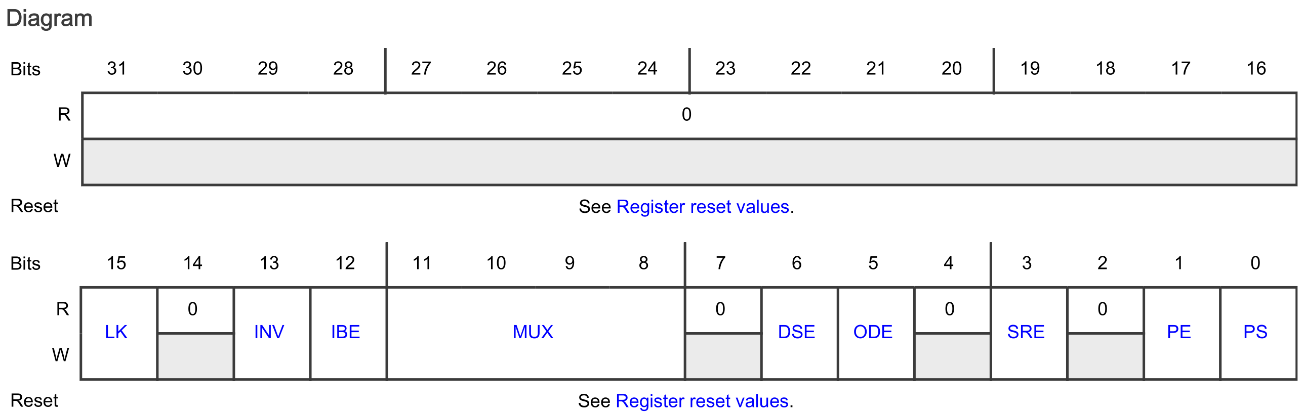
Each PORT contains up to 32 PCR registers. These registers all have the same layout, and are organized in an array. The PCR register for P3_13 is addressed as follows:
PORT3->PCR[13]
This register is used as follows for pin P3_13 to:
- Set the LK bit field to [1]: Lock this PCR
-
Set the MUX bit field to [0000]: alternative 0 (GPIO)
Refer to the reference manual paragraph 11.6, find Pin control a (PCR10 - PCR13), find the MUX bit-field description and make sure to understand why the alternative is set to 0 for GPIO.
-
Set all other bit fields to their reset value logic 0
// 1. & 2.
//
// Configure P3_13
// LK : [1] = Locks this PCR
// INV: [0] = Does not invert
// IBE: [0] = Disables
// MUX: [0000] = Alternative 0 (GPIO)
// DSE: [0] = low drive strength is configured on the corresponding pin,
//            if the pin is configured as a digital output
// ODE: [0] = Disables
// SRE: [0] = Fast
// PE:  [0] = Disables
// PS:  [0] = n.a.
PORT3->PCR[13] = 0x00008000;
3. Initialize P3_13 for output function
Refer to the reference manual paragraph 12.5. The following description is provided to initialize a pin for the output function:
// 1. Initialize the GPIO pins for the output function:
//    a. Configure the output logic value for each pin by using Port Data
//       Output (PDOR).
//    b. Configure the direction for each pin by using Port Data Direction
//       (PDDR).
// 2. Interrupt function not used.
Note: The interrupt function is not used in this example.
This description tells that there is a PDOR and PDDR register for the GPIO pins. For P3_13, these registers are addressed as follows:
GPIO3->PDOR
GPIO3->PDDR
Manipulating the 13th bit in these registers, manipulates pin P3_13. The following C instructions can be used, according to the description, to initialize P3_13 as an output pin:
// 1. a.
//
// PDO13: [1] = Logic level 1 – LED green off
GPIO3->PDOR |= (1<<13);

// 1. b.
//
// PDD13: [1] = Output
GPIO3->PDDR |= (1<<13);
Pin toggling
After initialization the pin can be toggled by using the PDOR register in the GPIO peripheral. Setting a bit in the PDOR can also be done by using the PSOR register. For resetting a bit in the PDOR register, the PCOR register can be used.
The following while-loop uses the PSOR and PCOR registers to create a blinking green LED:
while(1)
{
    // LED green off
    // Write logic 1 to bit 13 in the GPIO3 PSOR register so the
    // corresponding bit in PDOR becomes 1
    GPIO3->PSOR = (1<<13);

    // Delay
    for(volatile int i=0; i<1000000; i++)
    {}

    // LED green on
    // Write logic 1 to bit 13 in the GPIO3 PCOR register so the
    // corresponding bit in PDOR becomes 0
    GPIO3->PCOR = (1<<13);

    // Delay
    for(volatile int i=0; i<1000000; i++)
    {}
}
As mentioned, the same blinking functionality could have been achieved by using the PDOR register of PORT3. For example:
// Write logic 1 to PDOR bit 13
GPIO3->PDOR |= (1<<13);

// Write logic 0 to PDOR bit 13
GPIO3->PDOR &= ~(1<<13);
By using the PSOR and PCOR registers, there is no need to read the content of the PDOR register for updating a single bit. If the bitwise operators are used, there are three actions involved: Read-Modify-Write. Hence, this is not not an atomic action, and can thus be interrupted. Writing to the PSOR or PCOR register is an atomic action.
Another alternative for toggling a pin is by using the PTOR register. For example:
// Toggle the pin
GPIO3->PTOR = (1<<13);
Assignment
- Update the application so the red RGB LED blinks, instead of the green RGB LED.
- Update the application and initialize all the pins connected to the RGB LED as GPIO output.
- Update the while-loop to show the following sequence:
red -> green -> blue -> off -> red -> green -> blue -> off -> etc.
Extra
Create an LED chaser.
- Use a six LED breakout board, such as
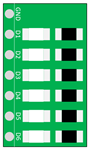
Alternatively, use six LEDs with suitable series resistors. Make sure the anode of the LED is connected to the microcontroller pin and the cathode to GND. Do not forget to add the series resistors.
- Connect the LEDs and the FRDM-MCXA153 board as follows:
| FRDM-MCXA153 | LED |
|---|---|
| GND | GND |
| P2_12 | D1 |
| P2_16 | D2 |
| P2_13 | D3 |
| P2_6 | D4 |
| P3_14 | D5 |
| P3_15 | D6 |
- In the file gpio_output.c correctly configure the pins so they can be used as GPIO output pins. Notice that PORT2 is also used.
TIP: There are two registers for MRCC_GLB_CC: MRCC_GLB_CC0 and MRCC_GLB_CC1. The same applies to MRCC_GLB_RST: MRCC_GLB_RST0 and MRCC_GLB_RST1. Refer to the reference manual to locate these registers and carefully verify where each module (PORT2, GPIO2, PORT3, and GPIO3) is enabled.
- After successfully configuring the pins, create an LED chaser in
main.c.
TIP: So far, delays have been created by for-loops. If you are curious about how to use a timer for that, you might want to take a look at the SysTick timer example. You can also import this example in the IDE from ese_driver_examples\systick\match_interrupt.