Standard Counter or Timer - PWM
Resources: ese_driver_examples\ctimer\pwm
Goal
Know how to use the standard counter or timer (CTIMER) module to generate a PWM signal.
CTIMER in PWM mode
The four 32-bit match registers in a CTIMER can be configured for PWM operation, allowing up to three single-edged controlled PWM outputs. The following timing diagram shows the interactions between the CTIMER value, the match registers and the output signal.
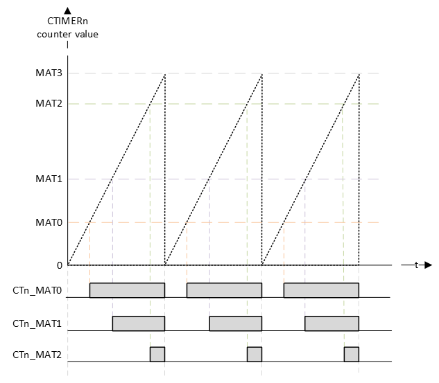
The timing diagram shows that the top value is the MAT3 register. The other MAT registers can be used for compare matches. If a match occurs, the corresponding pin will generate a rising edge. At the beginning of the PWM cycle, all channel pins will generate a falling edge (unless their match value is zero).
CTIMER configuration
The configuration of the CTIMER is done by following the initialization steps as described in the reference manual paragraph 26.1.5.
- Select a clock source for the CTIMER using MRCC_CTIMER0_CLKSEL, MRCC_CTIMER1_CLKSEL, and MRCC_CTIMER2_CLKSEL registers.
- Enable the clock to the CTIMER via the CTIMERGLOBALSTARTEN[CTIMER0_CLK_EN], CTIMERGLOBALSTARTEN[CTIMER1_CLK_EN], and CTIMERGLOBALSTARTEN[CTIMER2_CLK_EN] fields. This enables the register interface and the peripheral function clock.
- Clear the CTIMER peripheral reset using the MRCC_GLB_RST0 registers.
- Each CTIMER provides interrupts to the NVIC. See MCR and CCR registers in the CTIMER register section for match and capture events. For interrupt connections, see the attached NVIC spreadsheet.
- Select timer pins and pin modes as needed through the relevant PORT registers.
- The CTIMER DMA request lines are connected to the DMA trigger inputs via the DMAC0_ITRIG_INMUX registers (See Memory map and register definition). Note that timer DMA request outputs are connected to DMA trigger inputs.
As an example, a CTIMER1 will be used to create a PWM signal for dimming the red RGB LED to 10%. The PWM signal of will get a frequency of 1kHz. This doesn't require the use of interrupts or DMA requests, so steps 4. and 6. can be omitted. The other steps are explained in more detail in the following sections.
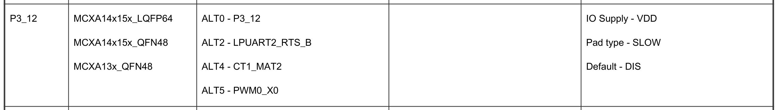
The red RGB LED is connected to P3_12. The reference manual shows that this pin is connected to CTIMER1 match register channel 2 (CT1_MAT2). This is mux alternative 4 (ALT4).
1. Select a clock source
The source clock is selected in the MRCC module. From the available options, 1MHz is selected. Furthermore, the source clock is configured to run and the divider is set to 1. This divider can be seen as an additional prescaler (available in the MRCC module).
// MUX: [101] = CLK_1M
MRCC0->MRCC_CTIMER1_CLKSEL = MRCC_MRCC_CTIMER1_CLKSEL_MUX(0b101);

// HALT: [0] = Divider clock is running
// RESET: [0] = Divider isn't reset
// DIV: [0000] = divider value = (DIV+1) = 1
MRCC0->MRCC_CTIMER1_CLKDIV = 0;
2. Enable the clock to the CTIMER
The CTIMER module interface and function clock are disabled by default. These are enabled in the SYSCON module as follows:
// CTIMER1_CLK_EN: [1] = CTIMER 1 function clock enabled
SYSCON->CTIMERGLOBALSTARTEN |= SYSCON_CTIMERGLOBALSTARTEN_CTIMER1_CLK_EN(1);
3. Clear the CTIMER peripheral reset
Similar to all other modules, the CTIMER needs to be enabled and released from reset in the MRCC module:
// Enable modules and leave others unchanged
// CTIMER1: [1] = Peripheral clock is enabled
MRCC0->MRCC_GLB_CC0_SET = MRCC_MRCC_GLB_CC0_CTIMER1(1);

// Release modules from reset and leave others unchanged
// CTIMER1: [1] = Peripheral is released from reset
MRCC0->MRCC_GLB_RST0_SET = MRCC_MRCC_GLB_RST0_CTIMER1(1);
5. Select timer pins and pin modes
By setting a prescaler of 10, the f_counter = 1 MHz / 10 = 100 kHz.
If the top (MAT3) value is set to (100-1), then f_pwm = 100 kHz / 100 = 1 kHz.
It also means that valid match register values are 0 to 100. So the precision of the PWM duty cycle is 100 steps.
Setting a duty cycle of 10% is done by writing 10 to the MAT2 register.
// Specifies the prescale value. 1 MHz / 10 = 100 kHz
CTIMER1->PR = 10-1;

// Match value: 100 kHz / 100 = 1 kHz
//
// In PWM mode, use match channel 3 to set the PWM cycle length. The other
// channels can be used for matches
CTIMER1->MR[2] = 10;
CTIMER1->MR[3] = 100-1;
Furthermore, the the three bits for each channel must be configured:
// MR2S: [0] = Does not stop Timer Counter (TC) if MR0 matches Timer Counter
//             (TC)
// MR2R: [0] = Resets Timer Counter (TC) if MR0 matches its value.
// MR2I: [0] = No interrupt when MR0 matches the value in Timer
//             Counter (TC).
// MR3S: [0] = Does not stop Timer Counter (TC) if MR3 matches Timer Counter
//             (TC)
// MR3R: [1] = Resets Timer Counter (TC) if MR3 matches its value.
// MR3I: [0] = No interrupt when MR3 matches the value in Timer
//             Counter (TC).
CTIMER1->MCR |= CTIMER_MCR_MR3R(1);
Plus the fact that PWM mode of operation is selected for channels 2 and 3:
// Configure match outputs as PWM outputs.
CTIMER1->PWMC |= CTIMER_PWMC_PWMEN3(1) | CTIMER_PWMC_PWMEN2(1);
The pin P3_12 must be configured for muxing slot alternative 4 as follows:
// Enable modules and leave others unchanged
// PORT3: [1] = Peripheral clock is enabled
MRCC0->MRCC_GLB_CC1_SET = MRCC_MRCC_GLB_CC1_PORT3(1);

// Release modules from reset and leave others unchanged
// PORT3: [1] = Peripheral is released from reset
MRCC0->MRCC_GLB_RST1_SET = MRCC_MRCC_GLB_RST1_PORT3(1);

// Configure P3_12
// LK : [1] = Locks this PCR
// INV: [0] = Does not invert
// IBE: [0] = Disables
// MUX: [0100] = Alternative 4 (CT1_MAT2)
// DSE: [0] = low drive strength is configured on the corresponding pin,
//            if the pin is configured as a digital output
// ODE: [0] = Disables
// SRE: [0] = Fast
// PE:  [0] = Disables
// PS:  [0] = n.a.
PORT3->PCR[12] = PORT_PCR_LK(1) | PORT_PCR_MUX(4);
And finally, the timer is enabled:
// CEN: [1] = Enables the counters.
CTIMER1->TCR |= CTIMER_TCR_CEN(1);
The theoretical result is depicted in the following timing diagram:
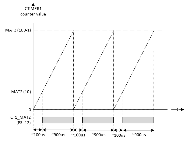
FYI: the RGB LEDs are on when the pin is logic 0.
Checking the actual generated signal with a logic analyzer:
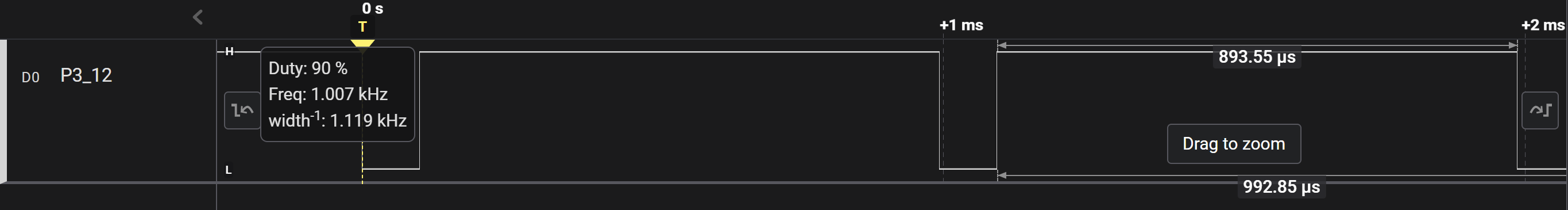
One thing to notice is that the CTIMER always generates inverted PWM signal (active low PWM)! In the example above this is not a problem, because the LEDs are on with logic 0. There is no configuration option to invert the generated PWM signal.
Assignment
Q1 In the example, the red LED was chosen and not the blue or green LED for a specific reason. Can you figure out that reason? Tip: look at the alternative functions of the pins.
Q2 What happens if you write 0 to MAT2?
Q3 What happens if you write 50 to MAT2?
Q4 What happens if you write 100 to MAT2?
Q5 What happens if you write 150 to MAT2?
Q6 What happens if the prescaler is changed from 10 to 1?
Q7 With the prescaler set to 0, what should be the value of MAT3 to maintain a 1 kHz PWM signal?
Q8 What is a benefit of a higher input frequency?