Assignment - EEPROM
Resources: ese_shieldv3_examples\eeprom\lpspi
Goal
To practice with the modules discussed so far.
Hardware requirements
- FRDM-MCXA153 board
- M950x0 EEPROM, available on Shield V3 or Mikroe-1200 add-on board
- Type-C USB cable
- Logic analyzer (optional)
Note. When using the Mikroe add-on board, different pins must be used and different instructions are applicable! Carefully study the datasheet of the used EEPROM on the add-on board.
Functional requirements
The application reads and writes from an external EEPROM. This is done through an SPI interface.
Architecture
The Shield V3 shows an example of how to connect the hardware parts.
EEPROM
EEPROM chips are devices that are controlled by sending instructions. One can think of an EEPROM, or any external device for that matter, as a microcontroller with very specific functions. It has internal registers that can be read and/or written through one of it's interfaces. In this case, the used interface is SPI.
The EEPROM datasheet shows a table with instructions. Some of these instructions are:
| Instruction | Description | Format bin | Format hex |
|---|---|---|---|
| WREN | Write enable | 0000 X110 | 0x06 |
| WRDI | Write disable | 0000 X100 | 0x04 |
| RDSR | Read Status register | 0000 X101 | 0x05 |
| WRSR | Write Status register | 0000 X001 | 0x01 |
| READ | Read EEPROM memory | 0000 0011 | 0x03 |
| WRITE | Write EEPROM memory | 0000 0010 | 0x02 |
In order to fully understand the devices features, one should carefully read the datasheet. Particular important are the reset values of the internal registers.
As an example, the following sequence diagram shows how the microcontroller can send the WREN instruction.
   LPSPI1             LPSPI1
   TXFIFO   EEPROM    RXFIFO
     ---      ---      ---
      |        |        |
      |  0x06  |        |
      +------->+        |
      |        |        |
The output of the EEPROM (MISO) is high impedance, so the value read by LPSPI1 should be ignored (RXMASK enabled).
A timing diagram with similar information is shown in the datasheet.
Here is another example for reading the RDSR instruction. Now the values read by LPSPI1 should not be ignored, however only the second values in the RXFIFO is actually considered a valid value.
   LPSPI1             LPSPI1
   TXFIFO   EEPROM    RXFIFO
     ---      ---      ---
      |        |        |
      |  0x05  |  0x00  |
      +------->+------->|
      |  0x00  |  0xF0  |
      +------->+------->|
      |        |        |
In this example:
- The LPSPI1 sends the RDSR (0x05) instruction. The EEPROM MISO pin is in high impedance state so 0x00 will be read by LPSPI1. This incoming byte should be discarded.
- The LPSPI1 sends dummy data (0x00 in the sequence diagram), and the EEPROM transmits the content of it's status register (0xF0), which can be read by LPSPI1.
A timing diagram showing similar information is shown in the datasheet.
API
In order to create the functional requirements, several API functions have already been prepared:
void lpspi1_wait_busy(void);
void lpspi1_tx(uint8_t *buffer, const uint32_t n, uint32_t rxmsk);
void lpspi1_rx_read(uint8_t *buffer, const uint32_t n);
void eeprom_init(void);
These functions can be used to implement the following API functions:
/*!
 * \brief Returns the content of the status register
 *
 * This functions sends the RDSR (0x05) instruction. After that, dummy data is
 * transmitted in order to receive the content of the 8-bit status register.
 *
 * \Return Content of the status register
 */
uint8_t eeprom_rdsr(void);

/*!
 * \brief Returns true if a write is in progress
 *
 * This functions reads the status register and returns true if the Write in
 * progress bit is set
 *
 * \Return true  WIP bit is set
 *         false WIP bit is not set
 */
bool eeprom_wip(void);

/*!
 * \brief Sets Write enable true or false
 *
 * Sends the write enable (WREN) or write disable (WRDI) to the EEPROM. Data
 * from the EEPROM is ignored.
 *
 * \param[in] wel true  WREN instruction is send
 *                false WRDI instruction is send
 */
void eeprom_we(bool wel);

/*!
 * \brief Reads n bytes starting at address
 *
 * This function fills the TXFIFO with the appropriate instruction and address.
 * A transfer is then initiated by calling the lpspi_tx() function as follows:
 * lpspi1_tx(NULL, 0, 0);
 * This will start the transfer of the instruction, address and n dummy bytes.
 * The result is copied into buffer by using the lpspi1_rx_read() function.
 *
 * \param[in]  address EEPROM start address
 * \param[out] buffer  pointer to store the data
 * \param[in]  n       number of bytes
 */
void eeprom_read(uint8_t address, uint8_t *buffer, const uint32_t n);

/*!
 * \brief Writes n bytes starting at address
 *
 * This function fills the TXFIFO with the appropriate instruction and address.
 * A transfer is then initiated by calling the lpspi_tx() function with the.
 *
 * \param[in]  address EEPROM start address
 * \param[in]  buffer  pointer to get the data
 * \param[in]  n       number of bytes
 */
void eeprom_write(uint8_t address, uint8_t *buffer, const uint32_t n);
Implement these functions. In main, these functions are already called to read/write from the EEPROM.
Some tips:
- While working on these functions, use a logic analyzer to visualize the data.
- When reading from the EEPROM, by default, all memory locations read 0xFF. Reading n bytes from the EEPROM means that the READ instruction and the address (see datasheet) must be transmitted first. This is depicted in the following sequence diagram.
   LPSPI1                              LPSPI1
   TXFIFO              EEPROM          RXFIFO
     ---                ---             ---
      |                  |               |
      | 0x03: READ inst. |  0x00: dummy  |
      +----------------->+-------------->|
      |                  |               |
      | 0x00: address    |  0x00: dummy  |
      +----------------->+-------------->|
      |                  |               |
      | 0x00: dummy      |  0xFF: data 1 |
      +----------------->+-------------->|
      |                  |               |
      | 0x00: dummy      |  0xFF: data 2 |
      +----------------->+-------------->|
      .                  .               .
      .                  .               .
      | 0x00: dummy      |  0xFF: data n |
      +----------------->+-------------->|
      |                  |               |
As an example: here is a timing diagram of reading the status register and four bytes from memory:
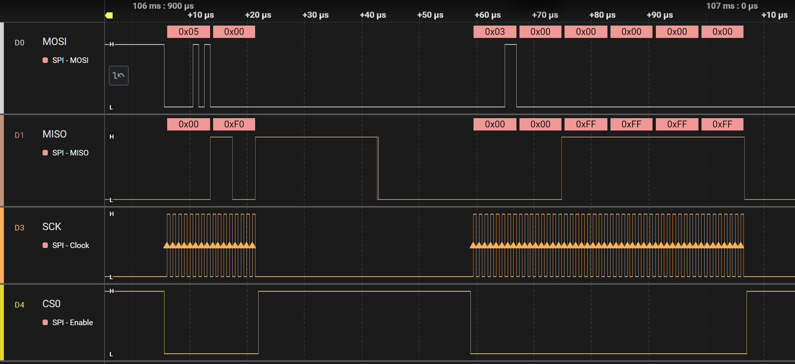
- Before writing to the EEPROM in main, make sure that writing is enabled with the eeprom_we() function. After writing is done, wait while a write is in progress with the eeprom_wip() function.