Low-Power UART - DMA
Resources: ese_driver_examples\lpuart\dma
Goal
To understand what DMA is.
To understand what it takes to use the LPUART with DMA.
Direct Memory Access
A Direct Memory Access (DMA) controller is capable of performing data transfers with minimal intervention of the host processor. This is depicted in the following simplified bus matrix diagram.
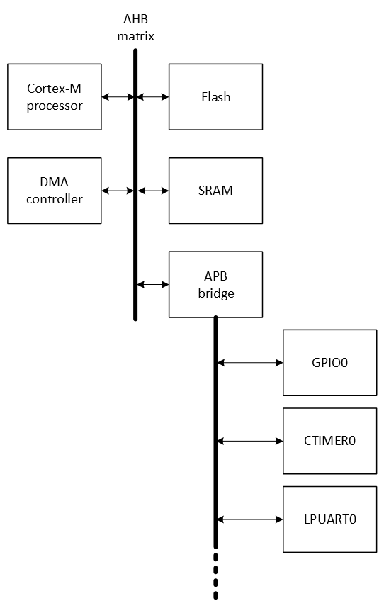
The Cortex-M processor is a master on the Advanced High-performance Bus (AHB). It initiates transfers from one location to the other. For example, when reading data from a UART register through the Advanced Peripheral Bus (APB), into a memory location in SRAM. This means that for simple tasks, such as moving data, the processor is busy.
Instead of letting the processor move data, the DMA controller can take care of that. This offloads the processor, so the processor can execute other instructions at the same time.
The reference manual paragraph 4.1 shows the more detailed bus matrix block diagram of the MCXA153 microcontroller:
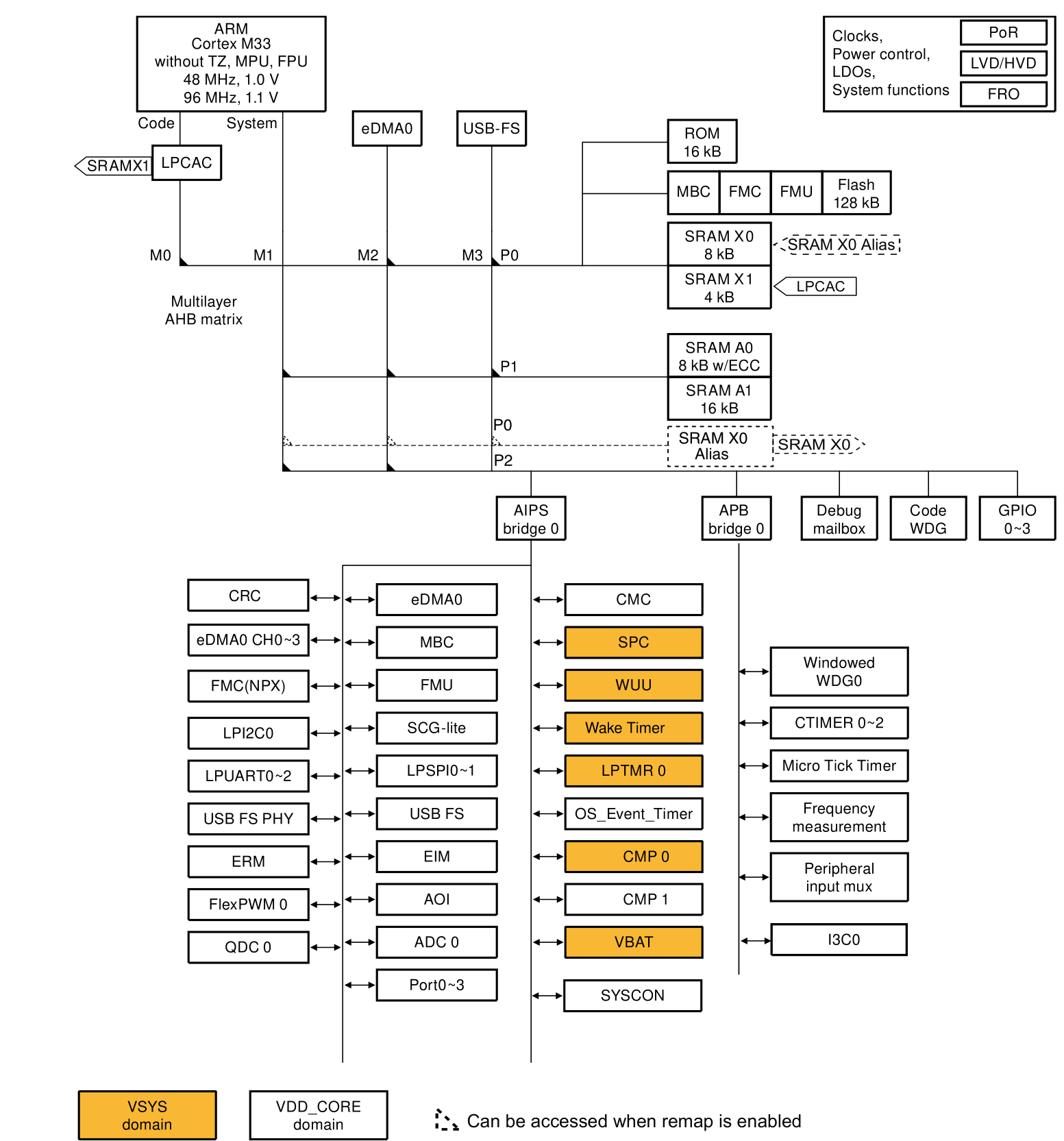
The figure shows a multilayer interconnection scheme that allows for parallel communication between multiple masters and slaves. Each master has its dedicated AHB layer that connects to all the slave devices. For a firmware developer this is transparent. In other words, the firmware developer can address a peripheral or a memory location by reading/writing a memory location.
Enhanced DMA Controller
The MCXA153 microcontroller has one so-called Enhanced DMA Controller (eDMA). It is described in chapter 15 of the reference manual.
The DMA controller is called eDMA0 and features four channels. This means it can be configured to move data from/to four source/destination pairs.
The eDMA module consists of two major subsystems:
- The eDMA engine
- The eDMA local memory that describes the transfer control for each channel. This is a.k.a. the Transfer Control Descriptors (TCD).
Features of the eDMA module are:
- Programmable source and destination addresses and transfer size
- Support for complex address calculations
- Internal data buffer, used as temporary storage for all transfers
- Channel activation via one of three methods:
- Explicit software initiation
- Initiation via a channel-to-channel linking mechanism for continuous transfers
- Peripheral-paced hardware requests, one per channel
- Channel completion reported via programmable interrupt requests
A simplified block diagram of the eDMA module is depicted below:
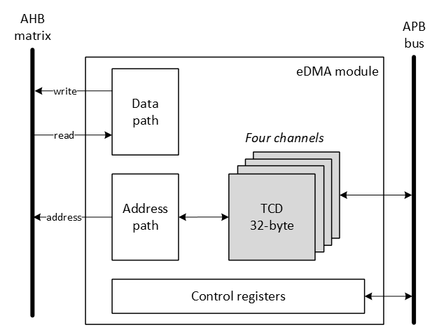
The eDMA module is configured through its Control registers and the four TCDs. Once configured, for each transfer it will:
- control the source and destination addresses
- read data from the source
- internally buffer the data if required
- write the data to the destination
- calculate the new source and destination addresses or optionally generates an interrupt when the transfer is finished
eDMA example: LPUART data transmission
This example demonstrates how to send a string of characters with the UART by using the DMA controller. Pins P0_2 (LPUART0_RXD) and P0_3 (LPUART0_TXD) will be used for UART signals. The DMA controller should generate an interrupt as soon as the transfer is finished.
The following needs to be configured initially:
- Enable modules
- LPUART0
- PORT0
- eDMA0
- Configure P0_2 and P0_3 pin functions
- Configure UART0
-
Associate the DMA channel with the UART0 peripheral. For this purpose, an Excel sheet is attached to the reference manual. It is called 'DMA_Configuration.xlsx'. Part of this table is depicted below:
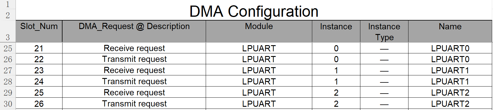
It shows, for example, that slot number 22 is the LPUART0 transmit request.
-
Enable channel interrupts
The following example shows the implementation for these steps for UART transmission with DMA channel 0.
void lpuart0_dma_init(const uint32_t baudrate)
{
    // Set clock source
    // MUX: [010] = FRO_HF_DIV (defaults: FRO_HF = 48 MHz; DIV = 1)
    MRCC0->MRCC_LPUART0_CLKSEL = MRCC_MRCC_LPUART0_CLKSEL_MUX(0b010);

    // HALT: [0] = Divider clock is running
    // RESET: [0] = Divider isn't reset
    // DIV: [0000] = divider value = (DIV+1) = 1
    MRCC0->MRCC_LPUART0_CLKDIV = 0;

    // Enable modules and leave others unchanged
    // LPUART0: [1] = Peripheral clock is enabled
    // PORT0: [1] = Peripheral clock is enabled
    // DMA: [1] = Peripheral clock is enabled
    MRCC0->MRCC_GLB_CC0_SET = MRCC_MRCC_GLB_CC0_LPUART0(1);
    MRCC0->MRCC_GLB_CC0_SET = MRCC_MRCC_GLB_CC0_PORT0(1);
    MRCC0->MRCC_GLB_CC0_SET = MRCC_MRCC_GLB_CC0_DMA(1);

    // Release modules from reset and leave others unchanged
    // LPUART0: [1] = Peripheral is released from reset
    // PORT0: [1] = Peripheral is released from reset
    // DMA: [1] = Peripheral is released from reset
    MRCC0->MRCC_GLB_RST0_SET = MRCC_MRCC_GLB_RST0_LPUART0(1);
    MRCC0->MRCC_GLB_RST0_SET = MRCC_MRCC_GLB_RST0_PORT0(1);
    MRCC0->MRCC_GLB_RST0_SET = MRCC_MRCC_GLB_RST0_DMA(1);

    // Configure P0_2
    // LK : [1] = Locks this PCR
    // INV: [0] = Does not invert
    // IBE: [1] = Digital Input Buffer Enable, otherwise pin is used for analog
    //            functions
    // MUX: [0010] = Alternative 2 - LPUART0_RXD
    // DSE: [0] = low drive strength is configured on the corresponding pin,
    //            if the pin is configured as a digital output
    // ODE: [0] = Disables
    // SRE: [0] = Fast
    // PE:  [0] = Disables
    // PS:  [0] = n.a.
    PORT0->PCR[2] = PORT_PCR_LK(1) | PORT_PCR_MUX(2) | PORT_PCR_IBE(1);

    // Configure P0_3
    // LK : [1] = Locks this PCR
    // INV: [0] = Does not invert
    // IBE: [0] = Input buffer disable
    // MUX: [0010] = Alternative 2 - LPUART0_TXD
    // DSE: [0] = low drive strength is configured on the corresponding pin,
    //            if the pin is configured as a digital output
    // ODE: [0] = Disables
    // SRE: [0] = Fast
    // PE:  [0] = Disables
    // PS:  [0] = n.a.
    PORT0->PCR[3] = PORT_PCR_LK(1) | PORT_PCR_MUX(2);

    // Configure LPUART0. Although there are a lot of configuration options, the
    // default configuration takes the following steps:
    // 1. Configure baud rate
    // 2. Enable receiver and/or transmitter

    // 1.
    //
    // Configure baud rate
    // OSR: [01111] = Results in an OSR of 16 (15+1)
    // SBR: [.............] = baud rate = baud clock / ((OSR + 1) * SBR)
    //                        => SBR = baud clock / (baud rate * (OSR+1))
    LPUART0->BAUD = LPUART_BAUD_OSR(0b01111) |
       LPUART_BAUD_SBR(CLK_FRO_48MHZ / (baudrate * 16));

    // 2.
    //
    // TE: [1] = Transmitter Enable
    LPUART0->CTRL |= LPUART_CTRL_TE(1);

    // Write a single time to this register, or it will be reset!!
    // In other words, do not update it in the function lpuart0_dma_write().
    // See 15.6.2.7:
    //     "If there is an attempt to write a mux configuration value that is
    //      already consumed by any channel, a mux configuration of 0 (SRC = 0)
    //      will be written"
    DMA0->CH[0].CH_MUX = DMA_CH_MUX_SRC(22);

    // Enable DMA channel 0 interrupts
    NVIC_SetPriority(DMA_CH0_IRQn, 3);
    NVIC_ClearPendingIRQ(DMA_CH0_IRQn);
    NVIC_EnableIRQ(DMA_CH0_IRQn);
}
For every transfer, paragraph 15.5.1 in the reference manual describes what should be done:
- Write to the MP_CSR if a configuration other than the default is wanted.
- Write the channel priority levels to the CHn_PRI registers and group priority levels to the CHn_GRPRI registers if a configuration other than the default is wanted.
- Enable error interrupts in the CHn_CSR[EEI] registers if they are wanted.
- Write the 32-byte TCD for each channel that may request service.
- Enable any hardware service requests via the CHn_CSR[ERQ] registers.
- Request channel service via either:
- Software: setting TCDn_CSR[START]
- Hardware: slave device asserting its eDMA peripheral request signal
Steps 1. to 3. are not required in a 'simple' UART requested DMA transfer. The other steps are explained in more detail in the following sections. An overview of what needs to be eabled is provided in the following image:
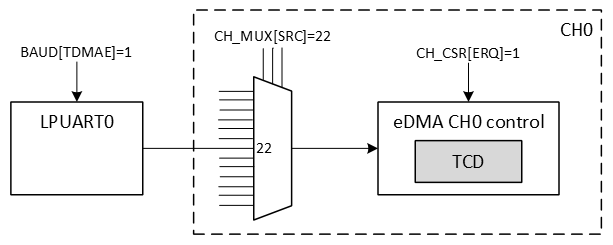
For a detailed description of a single request transfer, also see paragraph 15.5.5.1 of the reference manual.
4. Write the 32-byte TCD
The fields of the TCD are depicted in the following image (taken from the reference manual):
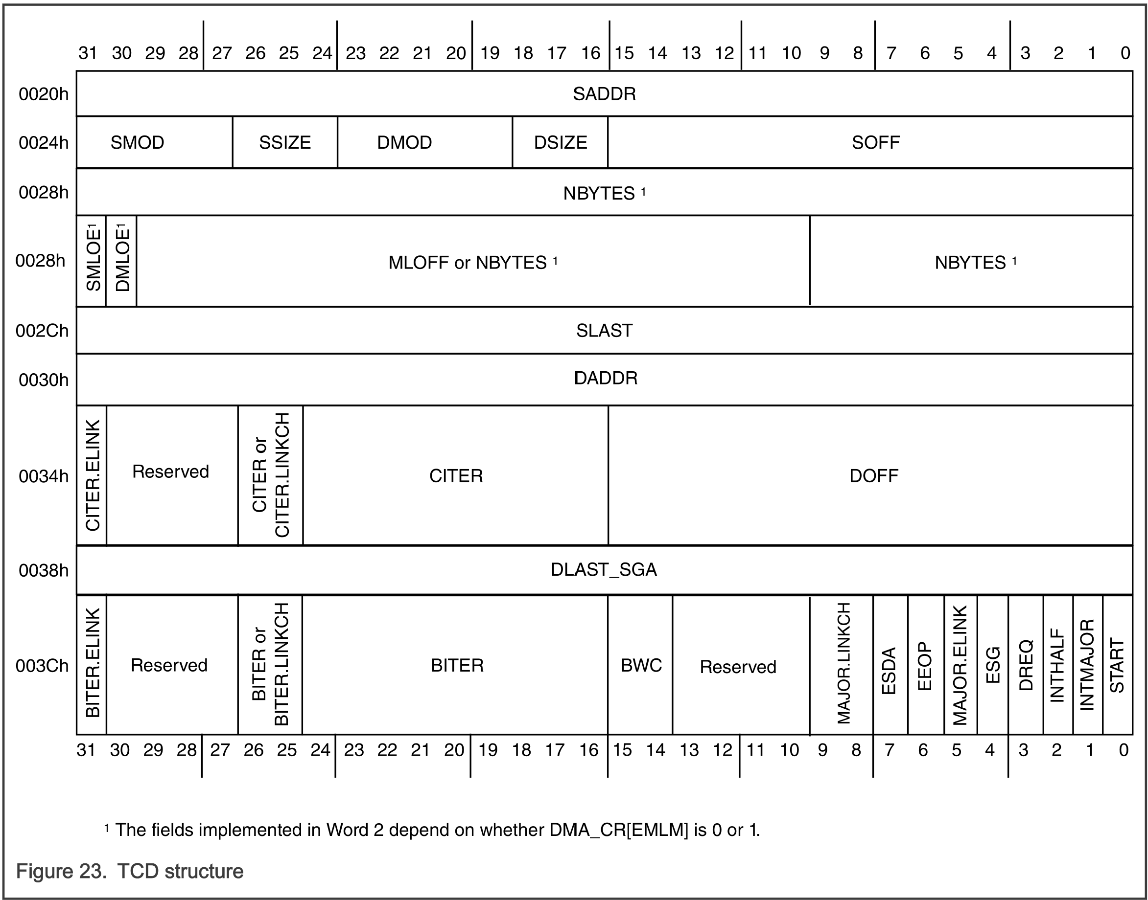
The following code snippet shows how to configure a transfer of n-bytes from a buffer in RAM to the UART data register:
// Source and destination address
DMA0->CH[0].TCD_SADDR = (uint32_t)buffer;
DMA0->CH[0].TCD_DADDR = (uint32_t)(&(LPUART0->DATA));

// Source address: +1
// Destination address: +0
DMA0->CH[0].TCD_SOFF = DMA_TCD_SOFF_SOFF(1);
DMA0->CH[0].TCD_DOFF = DMA_TCD_DOFF_DOFF(0);

// For both source and destination: modulo feature disabled and
// 8-bit transfers
DMA0->CH[0].TCD_ATTR = DMA_TCD_ATTR_SMOD(0) | DMA_TCD_ATTR_SSIZE(0) |
                       DMA_TCD_ATTR_DMOD(0) | DMA_TCD_ATTR_DSIZE(0);

// Transfer one byte per service request
DMA0->CH[0].TCD_NBYTES_MLOFFNO = 1;

// No address adjustments at the end of the major loop
DMA0->CH[0].TCD_SLAST_SDA = DMA_TCD_SLAST_SDA_SLAST_SDA(0);
DMA0->CH[0].TCD_DLAST_SGA = DMA_TCD_DLAST_SGA_DLAST_SGA(0);

// Major loop count (beginning and current): number of bytes
DMA0->CH[0].TCD_BITER_ELINKNO = n;
DMA0->CH[0].TCD_CITER_ELINKNO = n;

// Enable Interrupt if major loop count complete
DMA0->CH[0].TCD_CSR = DMA_TCD_CSR_INTMAJOR(1);
5. Enable any hardware service requests
The hardware service requests need to be enabled in the control registers of the eDMA (not the TCD).
DMA0->CH[0].CH_CSR |= DMA_CH_CSR_ERQ(1);
6. Request channel service
Channel service needs to be requested by the LPUART0, as soon as the transmit data register is empty. This is enable as follows:
// TDMAE : [1] = Enables STAT[TDRE] to generate a DMA request
LPUART0->BAUD |= LPUART_BAUD_TDMAE_MASK;
Interrupt handling
An interrupt handler is available for each channel. The following interrupt handler shows how to clear the interrupt flag, disable the UART transmit DMA request and set the global variable dma_write_done to indicate to the main application that the transfer is finished.
void DMA_CH0_IRQHandler(void)
{
    NVIC_ClearPendingIRQ(DMA_CH0_IRQn);

    DMA0->CH[0].CH_INT = DMA_CH_INT_INT_MASK;

    LPUART0->BAUD &= ~LPUART_BAUD_TDMAE_MASK;

    dma_write_done = true;
}
Assignment
None.